Well, I am quite excited to get the PuneChips forum up and running. While we would have liked to see more people attend, we had a good start. We invited most of the Semi/EDA folks in and around Pune and did get a very favorable response. Pending work and travel schedules are probably the culprits for a lower attendance, and I certainly hope that we will get more and more people to attend future events.
Ultimately, this forum is for the Semiconductor/EDA and Applications companies in and around Pune and we want to make sure that all future events/programs are catered to these companies needs. Again suggestions are most welcome and we are most certainly looking for individuals and companies to take on other responsibilities. We already have a taker for writing a guest blog so that is an encouraging sign.
That said I want to thank Abhijit Abhyankar from Rambus for taking time out of his busy schedule to present to us. The presentation was packed with lots of information generated a healthy amount of discussion during and after. Abhijit mentioned falling productivity and increasing power consumption as the two most important industry challenges, and therein lie the opportunities. Due to progressively declining geometries, number of transistors per chip has exploded, creating all sorts of new challenges. Conventional problem solving approaches are not working and radically different methodologies are required.

Ever since Gordon Moore made his empirical observation that transistor densities will double every two years, the industry has been making concerted efforts to ensure that Moore’s law remains valid despite all predictions otherwise. Physical limits do certainly pose a challenge to increasing the transistor densities in two dimensions, but scientists are working on 3D placement of transistors, where transistors are either placed vertically, or on top of each other. Another approach to increase densities is to skip the third dimension altogether and go directly to the fourth, i.e. Time. Some programmable device makers think that you can make a cell or logic block on the chip perform different functions during a clock cycle resulting in extremely dense chips without pushing physical limits. If these efforts are successful, Moore’s law will continue to live for a long time.
Interestingly, Google’s founder Sergey Brin came up with a new term coined “Page’s Law” (watch this clip) named after his co-founder just last month. It states that software gets twice as slow every 18 months, explaining why your cell phones and PCs seem slower even as the HW inside remains unchanged. This new law seems to be destined as a sidekick of Moore’s law and may provide a reason for people to go buy new hardware every 18 months! Maybe, this is what they call a virtuous cycle …
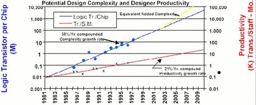
Jokes aside, productivity and power are certainly a couple of areas that need solving in the near term. SEMATECH or Semiconductor Manufacturing Technology Association has circulated this interesting chart which compares design complexities to designer productivity. This problem can certainly be solved by creating new tools that let the designer work from a much higher level than delving deep within the IC.
Additionally, today’s chips consume too much power. Power analysis has become a huge time sink during chip design due to very high densities. It may not be an overestimation to claim that power related issues are a major cause of productivity losses during chip design. Newer techniques that allow designers to work on reducing power from the early design stages are required, in addition to new architectures that inherently consume less power.
I personally feel that Indian companies should rise up to solve this challenge. While we are not well set as far as semiconductor manufacturing goes, we are certainly on the ball with respect to VLSI design, verification, simulation, etc. We have the talent, the training and now, even the experience to tackle these challenges. To all the young entrepreneurs out there, look at the evolving opportunities in this sector; there certainly is a world beyond web 2.0.
Finally big thanks to Kaushik Gala and the NCL Venture Center for opening up their facilities to this group. Rarely do we see such well equipped meeting rooms and fabulous campuses. I also want to thank everyone who attended the inaugural event. We had some very senior people attend from QLogic, LSI, and KPIT Cummins. There are 12-13 more companies in the area and I would really like to encourage engineers working there to attend. There will be lots of opportunities to learn from industry experts, network and formulate your ideas. Keep in mind that we will not be able to distribute yesterday’s presentation to a wider audience so those that did not attend truly missed out. I expect this will happen in the future due to corporate guidelines, so it is important that people show up for the event.
Once again, thanks to everyone who helped get PuneChips off the Ground.
If you’re a technology professional interested in the semiconductor/EDA area in Pune, please join the PuneChips mailing list and linked-in group.
About the Author – Abhijit Athavale
Abhijit Athavale is the President and CEO of Markonix, and a high-tech marketing consultant. He has 16+ years of high-technology industry experience. Prior to Markonix, Abhijit spent over 11 years at Xilinx, Inc. in various engineering, applications and marketing roles. In his role as a marketing consultant, he has held executive management positions at Taray, Inc and Sanved DA. He has a masters degree in electrical engineering from Texas A&M University and a bachelors degree in electrical engineering from University of Pune. He is an accomplished speaker and author of several publications including a book.
![Reblog this post [with Zemanta]](http://img.zemanta.com/reblog_b.png?x-id=a4c21947-3784-4a52-9a7e-294dced5fd90)
2 thoughts on “PuneChips Editor’s Blog: PuneChips Inaugural Event”
Comments are closed.