Tag Archives: EDA

Introducing http://PuneChips.com: The PuneTech SIG on Semiconductors, EDA, VLSI, Embedded Systems

Over the past 2 years, PuneTech has covered a breadth of technology related topics, with a concentration on Information Technology & Software. The strategic goal is to cover multiple technology segments and discuss innovative & exciting developments in these areas; specifically in Pune’s context.

It was with this objective that the concept of ‘SIG’ (Special Interest Group) was first mooted last year. A SIG covers a given vertical or horizontal domain area in depth. We decided that the best way to expand PuneTech would be to create a number of such SIGs, each focused on some particular vertical, and each run by someone who is passionate about that vertical. PuneTech would provide support, like a launching pad, publicity and visibility, and guidance about what works and what doesn’t work, based on our own experiences. Over time, we expect SIGs to have their own websites, and their own offline events.

PuneChips is a PuneTech special interest group on semiconductors, VLSI, embedded, and EDA. Click on the Logo to see all PuneTech articles about PuneChips

PuneChips was the first SIG, launched in June of 2009, launched by Abhijit Athavale (SIG Leader) in cooperation with PuneTech. It focuses on semiconductors design and applications. This SIG has arranged many successful meetings and events, and now it has also launched has its own website: www.punechips.com . This website features information about the PuneChips events, as well as blogs about the semiconductors and embedded system industry. Volunteers like Arati Halbe have helped with PuneChips (but more volunteers are needed). Also, the Venture Center and Kaushik Gala have been helpful in graciously providing their premises for holding PuneChips events. For more details see the PuneChips about page.

PuneTech hopes to incubate more SIGs like PuneChips in future, and spin them off as separate entities. PuneTech will continue to be actively involved in supporting and publicizing the events and activities of these SIGs. If you’d like to start one, please get in touch with us.

PuneChips Activities

Over the past 8 months, PuneChips has organized a number of interesting meetings, featuring senior thought leaders from the semiconductor industry. It also has an active google-groups mailing list and a ‘Pune Chips’ linkedin group. Nearly 200 professionals and students from the VLSI, Embedded Systems, and other related areas are members of these groups. You can also follow PuneChips on twitter.

The first kick-off meeting of PuneChips in June 2009 featured Abhijit Abhyankar, Head of Rambus India. His talk on Emerging opportunities in the semiconductor industry presented a nice overview of the semiconductor sector and its progression over the past few decades. He also discussed emerging opportunities and trends in this field.

The second event featured Shrinath Keskar, ex-MD of Ikanos India. His presentation: IC Design Challenges in the Telecom sector discussed the various challenges in IC Design, specifically with respect to the Telecom Sector.

The August 2009 speaker Jagdish Doma, former director of VLSI design Conexant Systems, covered ASIC Verification trends and challenges.

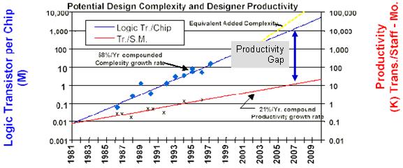
The October 2009 session featured a talk by Cliff Cummings, President of Sunburst Design and SystemVerilog Industry Guru. He talked about SystemVerilog & Designer Productivity, discussing specific tools and tricks for improving designer productivity.

The January session featured Madhu Atre, President of Applied Materials India. His talk on A Bright Solar Future discussed the various new developments in the area of solar power (specifically photo-voltaic) and the macro alternate energy global trends. He also touched upon the implications of these developments for India, including costs and government incentives.

In 2010, PuneChips plans to arrange similar meetings, featuring talks by thought leaders from the industry. The SIG also looks forward to more active interactions on the mailing list and linkedin group. If you are interested in learning more about the PuneChips activities and/or have a speaker you would like to recommend, please contact Abhijit Athavale.

You should form a SIG too – Get in touch with us

It would be great if Pune has many more such SIGs. A number of such groups and organizations are already active (some like the Pune Linux Users Group have existed long before PuneTech was started, and most like the Pune Open Coffee Club, for entrepreneurs and startups, were created independently). But there is scope for many more. The existing ones largely tend to be focused on particular technologies (like the Google Technologies User Group, or the Pune User Group for Microsoft Technologies). There are only a few that are aligned with industry verticals, like PuneChips or the Null group focused on security. I think there should be more.
So, if you’re passionate about some industry vertical, and are willing to spend at least a few hours a week on organizing a Pune-based SIG around that vertical, and are willing to do that for at least a couple of years, please let in touch with us, and let us make it happen.

In fact, it does not even have to be a vertical. It can be a horizontal area that goes across groups. As long as it is something that benefits Pune’s techies, we are game. In fact, we’re soon expecting to make an announcement related to PuneTech and Marathi. Subscribe to PuneTech so you don’t miss it.

PuneChips Editor’s Blog – SystemVerilog and Designer Productivity

The most recent PuneChips event was easily the most successful one in the short history of the group. Over 50 engineers attended the “SystemVerilog” talk by Clifford Cummings, President of Sunburst Design and SystemVerilog industry guru. A big thank you to a few folks who made this possible is in order; first off Parag Mehta of Qlogic for connecting us with Cliff; secondly in addition to Parag, Pravin Desale and Deepak Lala of LSI, and Jagdish Doma of Virage Logic for driving the attendance. Last, but not the least, we must also thank Cliff for taking us through a complex topic in a very engaging manner. Cliff certainly held the audience in rapt attention through an hour of highly technical discussion. The Q&A session was also very engaging. Of course, Cliff being the industry celebrity that he is, was mobbed by engineers asking questions after his speech.

It is very clear that SystemVerilog is clearly targeted at improving designer productivity. Failing productivity due to increasing design complexity is one of the biggest challenges faced by chip designers today, and it is not at all surprising that the EDA tool industry is focused on rectifying this. The chart below (source: SEMATECH) shows a rather grim picture – while design complexity has been growing at 58% CAGR, productivity has been increasing at only 21% CAGR. It is obvious to anyone that tools that fill this gap will be in great demand.

Failing Designer Productivity (Source: SEMATECH)

The reason for increasing design complexity is multifold – decreasing geometries allow designers to add more and more elements to the chip, making the entire process challenging. Number of IP cores per chip has grown from ~30 in 2003 to over 250 in 2006 and possibly much more today (source: EETimes). In addition, a big bull’s eye has been painted on power consumption numbers and most chips now must be designed using low power techniques. Plus, increasing complexity means that chip verification becomes more complex; 50% of all ASIC designs today require respins due to functional/logic errors (Source: Colette International Research).

Rather than a single solution, it is very likely that a multitude of innovative solutions that address individual problems will emerge. For example, better modeling techniques that can give a very accurate QoR estimate at the architecture stage itself can reduce the design complexity downstream. Languages such as SystemVerilog literally reduce the lines of code that a designer or verification engineer must write, thus boosting productivity. Time also may be right for ESL design, which has been around for a while, as conventional techniques fail to keep up.

All in all, we live in very interesting times. Faster and smaller is not always for the better. The industry must innovate and rise up to the economic and design challenges if it is to survive and prosper.

Reblog this post [with Zemanta]

PuneChips: Talk by Cliff Cummings on SystemVerilog FSM, Assertion, & RTL tricks for Design Engineers – 5 Nov

What: Talk by Cliff Cummings on SystemVerilog FSM, Assertion, & RTL Tricks for Design Engineers
When: Thursday, 5th November, 6:30pm to 8:00pm
Where: Venture Center, NCL Innovation Park, Pashan Road. To reach Venture Center, go past NCL towards Pashan, pass the cricket ground adjacent to NCL and then you’ll find NCL Innovation Park / Venture Center on the right hand side. Map
Registration and fees: This event is free for all to attend. No registration required.

The integrated circuit from an Intel 8742, a 8...
Click on the image to see all PuneTech articles about PuneChips. Image via Wikipedia

SystemVerilog FSM, Assertion, & RTL Tricks for Design Engineers

In the semiconductor and electronic design industry, SystemVerilog is a combined Hardware Description Language and Hardware Verification Language based on extensions to Verilog. As companies start migrating from Verilog to SystemVerilog it is becoming importatnt that they learn the tools of tread to effectively use it.

About the speaker – Cliff Cummings

Cliff Cummings is President of Sunburst Design, Inc., a company that specializes in world class Verilog, SystemVerilog and synthesis training. Mr. Cummings is an independent consultant and trainer with 27 years of ASIC, FPGA and system design experience and 17 years of Verilog, SystemVerilog, synthesis and methodology training experience. Mr. Cummings has completed many ASIC designs, FPGA designs and system simulation projects, and is capable of answering the very technical questions asked by experienced design engineers.

About PuneChips

PuneChips is a special interest group on semiconductor design and applications. PuneChips was formed to foster an environment for growth of companies in the semiconductor design and applications segment in the Pune area. Our goal is to build an ecosystem similar to PuneTech for companies in this field, where they can exchange information, consult with experts, and start and grow their businesses.

PuneChips has been started by Abhijit Athavale, president and CEO of Markonix, and a high-tech marketing consultant. He has 16+ years of high-technology industry experience. Prior to Markonix, Abhijit spent over 11 years at Xilinx, Inc. in various engineering, applications and marketing roles. In his role as a marketing consultant, he has held executive management positions at several companies. He has a masters degree in electrical engineering from Texas A&M University and a bachelors degree in electrical engineering from University of Pune. He is an accomplished speaker and author of several publications including a book.

For more information, see the PuneTech wiki profile of PuneChips, and/or join the PuneChips mailing list.

Please forward this mail to anybody in Pune who is interested in semiconductors, chip design, VLSI design, chip testing, and embedded applications.

Reblog this post [with Zemanta]

CORRECTION: ASIC Verification – guest post by Arati Halbe

Yesterday’s PuneTech post, “ASIC Verification: Trends and Challenges” was actually a guest post by Arati Halbe. Due to an oversight, I forgot to include the “About the Author” section in the post (in fact, I forgot to include any mention of the fact that the post was by Arati.) I apologize for the oversight.

Arati has close to 9 years experience in ASIC front end design and verification. Post silicon validation and FPGA prototyping is her recent area of interest and expertise. Arati has worked with Wipro Technologies and Conexant Systems. Arati did her B.E. from University of Pune and M.Tech from CEDT, Indian Institute of Science, Bangalore. See her linked-in profile for more details.

Reblog this post [with Zemanta]

ASIC Verification: Trends and Challenges

(This is a guest post for PuneTech by Arati Halbe, who has close to 9 years experience in ASIC front end design and verification. Post silicon validation and FPGA prototyping is her recent area of interest and expertise. Arati has worked with Wipro Technologies and Conexant Systems. Arati did her B.E. from University of Pune and M.Tech from CEDT, Indian Institute of Science, Bangalore. See Arati’s linked-in profile for more details.)

As the complexity of Integrated Circuits (specifically ASIC and SoC) increases, and as their sizes keep reducing, the task of testing the chip gets more and more challenging. Engineers need to come up with better and different methodologies to ensure what goes to the factory for manufacturing is actually what they intended to deliver. Verification occurs at various stages in the ASIC development cycle. How much is enough at each stage is a problem that needs to be addressed on a case to case basis. A sound knowledge of various techniques and awareness of capabilities and limitations of each technique goes a long way in making decisions about when, where and what.

The integrated circuit from an Intel 8742, a 8...
Click on the image to see all PuneChips articles on PuneTech. Image via Wikipedia

Keeping this in mind, PuneChips had verification expert Jagdish Doma talk about “ASIC verification: Trends and Challenges” on 20th August 2009. Though impacted by the H1N1 scare we had a small but diverse audience. Jagdish discussed in detail the strengths and limitations of the various techniques, viz: ESL, Formal verification, Dynamic simulation, FPGA prototyping and Emulation.

ESL or Electronic System Level testing is the newest trend. Supporters of ESL claim that it is a highly powerful system level modeling tool. It enables fast software bring-up if combined with an emulation/FPGA prototyping platform. ESL has been used successfully to validate systems for mobile applications where only one peripheral/application is active on the processor bus. ESL does not seem suitable for systems where multiple processes and interfaces are active simultaneously, like for example in a networking system.

Formal verification, a static verification technique which is mainly assertion based, is useful to check control paths. It cannot be used to verify datapaths. Dynamic simulation is a very effective way of verifying functionality of every block in the ASIC including the datapath. Gate level simulations performed after the back annotated placement and routing data is available are used to identify timing related issues or omissions/errors in stating multi-cycle paths.

The need to find hardware bugs as early as possible in the ASIC lifecycle drives the emulation and/or FPGA prototyping effort. Both these techniques enable the testing of scenarios which are generally not possible to test in dynamic functional verification, well before the actual silicon comes back from the fab. Emulation or prototyping also accelerate fast software ramp up and the software team can get a development platform ready well before the actual chip is available. Emulation involves running test cases on hardware accelerated platforms like Palladium from Cadence and Veloce from Mentor. For FPGA prototyping, Single or multiple FPGAs are used to build a PCB system targeted for the testing of the ASIC/SoC. The ASIC code is then fully or partially programmed on the FPGA/s and functionality can thus be tested.

Scenarios with much longer simulation times than what normal functional simulation allows can be run on the emulation platforms. All the internal signals are available for viewing and debug, just like in functional simulation. The FPGA prototype platform does enable longer test time, but the debugging available is limited. The hardware accelerators are costly, and investing in them makes sense if a company has lot of ASIC programs running simultaneously. For companies which have similar chips planned back to back, investing in a home grown FPGA based emulation/prototyping platform makes sense. Another advantage FPGA prototyping is that the RTL goes through a complete synthesis and place and route cycle and testing is done on a circuit which is as close to the real ASIC as possible.

To ensure that a bug free product reaches the customer is a complex activity and poses multiple challenges. Coverage, legacy code, repeatability are issues that need to be tackled. Ensuring that the coverage is at an acceptable level is important. Code coverage is run to find out if all the possibilities of a written code are exercised in a test suite. Simulators from cadence (ius), synopsys(vcs) and mentor (modelsim) have their own code coverage analyzers. Functional coverage means to find out if each feature listed in the specification for an ASIC/SoC is verified. It is essential that the functional specification document has an individual numbered paragraph for each feature so that traceability is easier. Functional coverage is an activity that needs planning, reviews and careful test case designing. Methodologies like eRM (e reuse methodology – Specman based) and OVM (open verification methodology – System verilog based) do assist checking functional coverage, but the inputs provided need careful specification and reviews.

Reviews, not just for coverage, but at every stage in the ASIC cycle are extremely important. One of the challenges encountered while designing an ASIC is that the hardware team interprets a certain behavior from software and the software expects that certain things are taken care of in hardware. It is very important to involve members from design team, verification team, architecture team, software & firmware team for verification review.

It takes a good amount of effort to come up with a verification environment, and it is very common for a team to use what has worked before when schedules are demanding. Legacy environment saves lot of time, but it also handicaps the team. Talking about saving time, efficiency goes a long way in shrinking the schedules. The initial time and effort investment in automation of repetitive tasks save lot of time in future. Use of re-usable methodologies will definitely save time and effort.

Finally, while choosing the verification flow for a certain ASIC, team needs to look at what is available in terms of resources as well as time, understand the end user requirement, and make a decision on which technique to employ at what stage.

Reblog this post [with Zemanta]

PuneChips Event: ASIC Verification trends and challenges – Jagdish Doma, former director of VLSI design Conexant Systems – 20 Aug

The integrated circuit from an Intel 8742, a 8...
Image via Wikipedia

What: Trends and Challenges by Jagdish Doma, former director of VLSI design for Conexant Systems
When: Thursday, 20th August, 6:30pm to 8:00pm
Where: Venture Center, NCL Innovation Park, Pashan Road. To reach Venture Center, go past NCL towards Pashan, pass the cricket ground adjacent to NCL and then you’ll find NCL Innovation Park / Venture Center on the right hand side. Map
Registration and fees: This event is free for all to attend. No registration required.

ASIC verification – Trends and Challenges

Jagdish will discuss the ASIC verification flow, various verification and validation techniques, and strength areas and limitations of each technique and the key challenges faced by companies during the ASIC verification cycle.

About the speaker – Jagdish Doma

Jagdish served as Director of VLSI Division for Conexant Systems in Pune where he was responsible for managing diverse teams involved in design, verification, validation, implementation, physical design and software development. During his 19 year career, Jagdish has held various senoir techical positions at Texas Instruments, Cirrus Logic and AMD. He brings a wide range of experience in Architecture, Design, pre-silicon verification, post-silicon validation and leading organizations to successful product development. Jagdish holds Bachelor’s in Electrical Engineering from University of Pune and a Master’s in Electrical Engineering fromTexas A&M University.

About PuneChips

PuneChips is a special interest group on semiconductor design and applications. PuneChips was formed to foster an environment for growth of companies in the semiconductor design and applications segment in the Pune area. Our goal is to build an ecosystem similar to PuneTech for companies in this field, where they can exchange information, consult with experts, and start and grow their businesses.

PuneChips has been started by Abhijit Athavale, president and CEO of Markonix, and a high-tech marketing consultant. He has 16+ years of high-technology industry experience. Prior to Markonix, Abhijit spent over 11 years at Xilinx, Inc. in various engineering, applications and marketing roles. In his role as a marketing consultant, he has held executive management positions at several companies. He has a masters degree in electrical engineering from Texas A&M University and a bachelors degree in electrical engineering from University of Pune. He is an accomplished speaker and author of several publications including a book.

For more information, see the PuneTech wiki profile of PuneChips, and/or join the PuneChips mailing list.

Please forward this mail to anybody in Pune who is interested in semiconductors, chip design, VLSI design, chip testing, and embedded applications.

Reblog this post [with Zemanta]

Too Soon to call for a Semiconductor Recovery?

(This post by Abhijit Athavale, the driving force behind PuneTech’s PuneChips forum, is cross-posted from his blog.)

Are we really out of the most dreaded recession after the great depression and on our path to recovery? The answer might be a resounding yes if we look at the recent crop of earnings reports from technology companies, and other data emerging from market analysis firms. In fact, the NASDAQ composite is already into deeply positive territory on the expectations of an imminent recovery.

Revenue and Inventory Declines from 2008 to 2009

However, a quick dissection of recent earnings announcements from a few prominent semiconductor companies shows that we are not out of the woods yet. The chart above shows that sales numbers are still horribly bad compared to last year, and inventories have declined sharply as well. This means that companies have managed to satisfy the underlying demand by using up their inventories, and will or already have started ordering replacement units from fabs. This explains why the fabs have reported better numbers than the IC vendors. In a normal growth phase, every company wants to keep its channel well stocked to feed demand. This is not the case now as companies are drawing down on finished stock to reduce costs and improve margins. So much for the expected recovery in demand …

Where does this demand come from ultimately? The consumer, of course. The US, Europe (as a whole) and Japan are the three largest economies in the world.

People living in these countries constantly keep (or, at least used to) buying new things such as laptops and PCs, cell phones, gaming consoles, automobiles, audio and video equipment, personal media players, TVs, toys, and other gadgets. Companies that manufacture consumer electronics ICs directly feed this demand. Consumers also buy services such as wireless and wireline voice and data, broadband, cable and satellite TV feeds. This in turn generates demand for the entire telecom, datacom and wireless infrastucture and service providers. Infrastructure IC manufacturers are responsible for suppplying this demand. In the US alone, the consumer is 70% of the entire economy. The consumer is also a major portion of the EU and Japanese economies. The consumption in all three major economies in the world has cratered, as evidenced by the continuous 6 to 9 month declines in the exports from China, Taiwan and Japan, major export reliant countries.

The real demand will not be back till the consumer starts spending again. And, that is almost impossible in this economy. Take the US for example – official unemployment is at ~11% (some say, it is near 16% unofficially), one in ten homeowners is underwater, and credit lines have been severely downgraded by banks. Three major sources of funds used by consumers have been seriously compromised. To use a banking term, the consumer is now de-leveraging and getting his house in order. There will be no more spending sprees till the US savings rates are back to historical levels. The EU and Japan are in even worse situations as their banks are still over leveraged and that still needs to be played out a la Bear Sterns and Lehman Brothers.

My belief is that the semiconductor industry and the companies that serve the semiconductor industry are not coming back till personal finances get better. That is not likely to happen for a while. Some analysts are calling Q2, 2009 as the bottom, which very well may be so, but I don’t expect to see a quick recovery from this point on. In fact, the worsening unemployment and foreclosure numbers may push us back into a double dip recession. If not, the recovery will be tepid and totally unspectacular.

Reblog this post [with Zemanta]

PuneChips Editor’s Blog – Second Edition

First, an update on PuneChips – we now have 5465 members in the Linked In group and over 40 in the Google Groups mailing list. Some folks doing applications work have also joined us. Given that there are 300 or so semiconductor designers in the Pune area, and hundreds more developing applications, we have ways to go.

On Monday, June 29th, we had our second event; a speech by Shrinath Keskar, former M.D. of Ikanos Communications in India. A good cross section of people attended the event and the discussion was quite lively. We had several new faces in the room, a definitive indicator of progress.

We also have our first guest blog written by Chaitanya Rajguru of KPIT Cummins Infosystems, and this is really what we are looking for. I want more people to participate in group discussions and idea generation. Rather than having only just a handful of people writing content, involvement from all is needed if we want to keep growing and have a voice in the development of Pune as a Chip/Embedded design hub.

Shrinath spoke about the challenges of designing chips for the telecom sector. The topic was quite relevant since we have several companies in the area that service Telecom applications. Shrinath not only focused on design challenges which generally revolve around the cost/power/features triangle, but also on challenges offered by the market; telecom standards, time to market and deployment. This was good information for engineers as it explained the logic behind many management decisions.

Telecom standards, both wireline and wireless, drive how telecom companies go about their business. Standards not only have technical, but regulatory challenges associated with them. In addition, there are competing standards that try to solve the same problem (Fig 1) and technical slugfests go on for many years before a winner emerges.

Figure 1: Plethora of Wireless Standards, Source: Nokia

Many a times, the winning standard has such a short window of opportunity that it may be pointless to keep designing to it. Sometimes, governments propose standards in order to get access to advanced technology; China proposed WAPI a few years ago for wireless security. The catch was that anyone trying to sell Telecom equipment in China would have to disclose their technology to a Chinese partner if (emphasis is mine) WAPI had been adopted.

In order to support current and possibly future standards, chips have to be intelligently designed with possibly some redundant I/O, memory and cells which can be used to fix design faults or adapt to changing standards. Figure 2 below shows what a chip designer spends doing day in and out and to Shrinath’s point, there are lots of opportunities available for innovators to improve the design process – innovation does not need to end at the transistor level.

Figure 2: Where a Designer Spends All His Time, Source: Xilinx, 2004

Telecom equipment typically stays in the market for years as telecom standards take a while to roll out due to regulatory or geographical hurdles. However, a chip vendor hardly ever has that kind of time to supply the product. A telecom line card will be generally designed in 9-12 months and the chip must be designed, tested and deployed in the production line card within that timeframe. Time to Market is very important for Telecom OEMs; hence chip vendors must be able to convert design wins into production chips that work.

Deployment is a very important phase in the life of a telecom chip. You can test the product in labs that mimic customer test environments, but you can never test for real situations such as interference from out of spec frequency bands. It is very important to have good support staff on hand to fight these battles alongside customers. Your chip must work in each and every deployment; even a 90% success rate will not cut it.

As Moore’s law comes to the end of life, there is a lot of discussion happening around a new sustainable model for chip startups. The current model, which requires upwards of $50M in VC money to be profitable, cannot live for long. Very likely, the next invention in the semi/EDA market is going to be economic, something that allows new companies to form and prosper.

Abhijit Athavale
PuneChips Editor

Reblog this post [with Zemanta]

How green will be my valley?

(This is a guest blog by Chaitanya Rajguru, Associate Technical Fellow at KPIT Cummins, and a member of the PuneChips group.)

The integrated circuit from an Intel 8742, a 8...
Image via Wikipedia

The “greening” of all things commercial and industrial is all around us. Every industry from transportation to technology to power to finance is in a rush to be perceived as “green”. So should the EDA industry stay behind? I think not. And here are my thoughts on some possible scenarios on what may happen.

So where does one begin? One good starting point may be with a popular indicator used to gauge the “goodness” of EDA tool’s output: “Quality of Results”, or QoR. QoR is used as a higher-level indicator of process quality, much like a Customer Satisfaction Index that up-levels feedback on specific aspects such as timely delivery and responsiveness. IC design EDA tools have used to showcase what they can do. So is it possible to expand its scope to include “greenness” as well? Or is it just an attempt to paint a turkey blue and pass it off as a peacock?

QoR is one of the long-lived and often-used keywords in Silicon Valley – surely on par with “information superhighway” in sheer citation count. Yet the latter phrase isn’t heard much anymore. It just reminds us of the 90’s internet boom, and doesn’t convey anything that is new today. After all, this superhighway is now as much part of our lives as electric power distribution is, and it has been a while since either created much excitement. And so is “QoR” similarly frozen in time as well, not staying up-to-date with today’s design challenges?

Let us take a quick look at how QoR has evolved over time. In the early days of IC design, the biggest challenge was to pack as many transistors onto a single die as possible. The self-fulfilling prophecy of Moore’s Law had setup expectations that somehow had to be met! And while the accompanying frequency spiral required lots of efforts to maintain, it was achievable. Thus the QoR directly reflected “transistor count” and “frequency” as the most important indicators of EDA tool capability. Other variations appeared, such as the packing density of logic and analog circuitry.

“Power” then appeared on the QoR scene, as limits of battery power and even socket power were approached by systems. Now EDA vendors could speak the language of the system architects with their “power-performance-area” optimization triangle. Higher-level performance metrics such as MIPS and FLOPS entered. Then came combinations such as “MIPS per megahertz per watt.” Thus the QoR definition expanded from the “micro” qualities to encompass the “macro”: from frequency and packing density to power and performance.

Looking at current trends in the economy, “Going Green” has taken on big importance everywhere. It is the socio-politically correct thing to do, regardless of your product or service. Companies with physical products joined the bandwagon early: building architects, automobile manufacturers, consumer electronics OEMs, and IC manufacturers. One software company that has made a start is Google, with its goal to “minimize its carbon footprint.” Other companies have been slower to adapt – maybe due to having “soft products,” or maybe because they find it hard to make the right connection into this trend. But the semiconductor industry and the EDA industry are inevitably subject to the same greening trend, and can not convincingly “opt out.”

But “Being Green” is as high-level a quality metric for an EDA product as any – so much so, that whether it even applies to EDA tools is sure to be hotly debated. Yet suppose, for a moment, that it were to be made a part of QoR, how do you think it can be done?

Initial thoughts that come to my mind suggest getting a “Green Process” certification for the EDA tool development cycle, analogous to the ISO9001 or CMMI certifications. In the future, such certifications could surely be applicable to any business or organization (maybe even an individual!), and the EDA industry would be no exception. Another possibility is to publish a “carbon footprint” or “carbon neutrality indicator.”

But the above “green indicators” apply only to the development of the EDA tools, and give no satisfactory indication of whether their use will lead to “green products”. My best suggestion so far to gauge that quality is to measure the tool performance (the fewer compute cycles it burns, the better) and its reuse (the more, the better). Reuse can be in terms of reusing the building blocks (within a project), the output (across projects) and even the hardware utilization (e.g. exploiting multicore architectures). I believe these quality measures will anyway be applied to the evaluation of EDA tools, because they also affect development cost and schedule. So one might as well explicitly go after these indicators and kill two birds in one stone!

On the downside of a green QoR, we could be chasing a red herring. Isn’t it be better to focus on the core job of the EDA tool, which is to make the design task easier? To what extent do we go in order to conform to this latest fad? And how about degrees of greenness, and who measures those? If two tool vendors claim to be green, how do I verify their claims and compare them against each-other?

So, what do you think about the “Greening of QoR?” Is it meaningful? If not, why not? And if yes, how can we go about it? It’s always fun to make predictions, so please do share yours …

About the Author – Chaitanya Rajguru

Chaitanya is an Associate Technical Fellow at KPIT Cummins Infosystems Ltd. He has extensive experience in end-to-end development of semiconductor products, from definition to production, with specialization in PC chipset, graphics and Flash memory IC products. He has played various roles such as product development lead, technical expert, people manager and organizational development facilitator.

Reblog this post [with Zemanta]

Event: IC Design Challenges in the Telecom sector – Shrinath Keskar, ex-MD Ikanos, India – 29th June

The integrated circuit from an Intel 8742, a 8...
Image via Wikipedia

What: Talk by Shrinath Keskar, fomer MD Ikanos Communications India, on IC Design Challenges in the Telecom Sector.
When: Monday, 29th June, 6:30pm to 8:00pm
Where: Venture Center, NCL Innovation Park, Pashan Road. To reach Venture Center, go past NCL towards Pashan, pass the cricket ground adjacent to NCL and then you’ll find NCL Innovation Park / Venture Center on the right hand side. Map
Registration and fees: This event is free for all to attend. No registration required.

About the speaker – Shrinath Keskar

Shrinath Keskar, former M.D. of Ikanos Communications of India has over 17 years of experience in the field of Semiconductors. He joined Ikanos in the year 2000 and has been with the company since then. Shrinath also worked with Fortune 500 hindered companies such as Motorola and Sun Microsystems before joining Ikanos. He has a Master’s degree in Computer Engineering from Texas A &M and B.E. from College of Engineering, Pune.

About PuneChips

PuneChips is a special interest group on semiconductor design and applications. This event is the inaugural event for PuneChips. PuneChips was formed to foster an environment for growth of companies in the semiconductor design and applications segment in the Pune area. Our goal is to build an ecosystem similar to PuneTech for companies in this field, where they can exchange information, consult with experts, and start and grow their businesses.

For more information, see the PuneTech wiki profile of PuneChips, and/or join the PuneChips mailing list.

Please forward this mail to anybody in Pune who is interested in semiconductors, chip design, VLSI design, chip testing, and embedded applications.

Reblog this post [with Zemanta]