Gouri Agtey Athale has an interesting article in the Pune Mirror pointing out that following the success of the “animation and gaming” niche sector, the IT industry in Pune should start focusing on other niche sectors – for example electronic design.
Excerpts:
[The] niche area of animation and gaming has worked out for Pune the way the software industry worked on the existing industrial base: combining the existing dormant and untapped potential and build a whole new business out of it.
Pune’s arrival on the animation and gaming scene has received recognition at the international level: two animation films made by companies based in Pune have made it to the list of Oscar nominations, Krayon’s Delhi Safari and Reliance Big’s Krishna and Kaunsa.
and
That was in the past: the move now is to move on and the next wave could be a convergence of the hardware and software sectors to create ESDM, or Electronic System Design and Manufacturing. Cmde (retd) Anand Khandekar, former member of the IT committee of the MCCIA, who helped draft the state’s IT policy over a decade ago, suggested that existing expertise in embedded software and the presence of the hardware sector in the city could be married to the city’s industrial culture and the educational base to create an industry around ESDM.
The blue print that ESDM is looking at is that of the automotive sector, where there are vendors who supply to the original equipment manufacturer, the OEM. On these lines, local entities could become vendors to global companies, the example usually cited being that of Taiwanbased companies who work on projects for global majors like Apple, Oracle-Sun Micro and Google- Motorola.
and finally:
And the sector needs a champion, a strong, non-partisan platform, which in the case of Pune’s software industry was the MCCIA.
(This report of an demo/event organized by NVidia in February 2012 was written by Abhijit Athavale, and was originally published on PuneChips.com, a PuneTech sister organization that focuses on semiconductor, eda, embedded design and VLSI technology in Pune. It is reproduced here for the benefit for PuneTech readers.)
I was invited to visit the Nvidia Tech Week this past weekend (February 25-26, 2012) at their facilities in Pune. This is a great concept – getting employees to invite friends and relatives to actually see what their company is all about is very good social outreach and a fantastic marketing initiative. If more tech companies in the area do similar events once or twice a year, it will help lift the shroud of technical opaqueness around them. I think hosting similar events in area colleges will also help students realize that even VLSI/Embedded Systems Design is cool.
I was given a personal tour by Sandeep Sathe, a Sr. Development manager at Nvidia and also met with Jaya Panvalkar, Sr. Director and head of Pune facilities. There was enough to see and do at this event and unfortunately I was a bit short on time. It would have taken a good two hours for a complete walk-through, so I decided to spend more time on the GPU/HPC section though the Tegra based mobile device section was also quite impressive. It’s been a while since I actually installed a new graphics card in a desktop (actually, it’s been a while since I used a desktop), but graphics cards have come a long way! Nvidia is using standard PCI Express form factor cards for the GPU modules with on-board fans and DVI connectors.
The following are key takeaways from the demo stations I visited
GeForce Surround 2-D
Here, Nvidia basically stretches the game graphics from a single monitor to three monitors. Great for gamers as it gives a fantastic feel for peripheral vision. The game actually doesn’t have to support this. The graphics card takes care of it. The setup here is that while the gamer sits in front of the main monitor, he also sees parts of the game in his peripheral vision in two other monitors that are placed at an angle to the main monitor. I played a car rally game and the way roadside trees, objects moved from the main monitor to the peripheral vision monitors was quite fascinating.
GeForce 3-D Vision Surround
This is similar to the above, but with 3D. You can completely immerse yourself in the game. This sort of gaming setup is now forcing monitor manufacturers to develop monitors with ultra small bezel widths. I suppose at some point in the next few years, we will be able to seamlessly merge graphics from different monitors into one continuous collage without gaps.
Powerwall Premium Mosaic
Powerwall is a eight monitor setup driven by the Quadro professional graphics engine. Two Quadro modules fit into one Quadroplex industrial PC to drive four monitors. Projectors can also be used in place of monitors to create a seamless view. The display was absolutely clear and highly detailed. The Powerwall is application transparent. Additional coolness factor – persistence data is saved so you don’t lose the image during video refresh and buffer swaps. This is most certainly a tool intended for professionals who need high quality visuals and computing in their regular work. Examples are automotive, oil and gas, stock trading.
PhysX Engine
PhysX is a graphics engine that infuses real time physics into games or applications. It is intended to make objects in games or simulations move as they would in real life. To me this was very disruptive, and highlight of the show. You can read more about PhysX here. It is very clear how PhysX would change gaming. The game demo I watched had several outstanding effects: dried leaves moving away from the character as he walks through a corridor, glass breaking into millions of shards as it would in real life. Also running was a PhysX simulation demo that would allow researchers to actually calculate how objects would move in case of a flood. What was stunning was that the objects moved differently every time as they would in real life. PhysX runs on Quadro and Tesla GPUs. It is interesting to note that Ra.One special effects were done using PhysX.
3D photos and movies
Next couple of demos demonstrated 3D TV and photo technology using Sony TVs and a set of desktops/laptops. Notably, the Sony 3D glasses were much more comfortable compared to others. Nvidia is working with manufacturers to create more comfortable glasses. There was also a Toshiba laptop that uses a tracking eye camera to display a 3D image to the viewer regardless of seating position without glasses. It was interesting. However, the whole 3D landscape need a lot of work from the industry before it can become mainstream.
Optimus
What was explained to me was that Optimus allows laptops to shut off GPUs when they are not needed. They can be woken up when high performance work is required. This would be automatic and seamless, similar to how power delivery is in on a Toyota Prius. This sort of a technology is not new to computing – a laptop typically puts a lot of components to sleep/hibernate when not being used, but the GPU is not included.
Quadro Visualizations
This allows 2D/3D visualizations for automotive, architectural and similarly complex systems for up to one thousand users at a time. You can easily change colors, textures, views so everyone can comment and give constructive feedback. I was not sure if the design can be changed on the fly as well. Nvidia is working with ISVs like Maya and Autodesk on this.
Tesla
Tesla GPUs use chips that are used for high performance computing and not rendering, which is different from what Nvidia typically does. The Tesla modules do not have any video ports! It has a heterogeneous GPU/CPU architecture that saves power. In fact, the SAGA-220 supercomputer, dubbed India’s fastest, at ISRO’s Vikram Sarabhai Space Center facility uses 2070 Tesla GPUs along with 400 Intel Xeon processors. In addition to supercomputing, Tesla is very useful in 3D robotic surgery, 3D ultrasound, molecular dynamics, oil and gas, weather forecasting and many more applications.
Tegra Mobile Processor
Next few demos showcased the Tegra mobile applications processor based on ARM Cortex A9 cores. The HD quality graphics and imaging were impressive. It is clear that smartphones and tablets of the day are clearly far more powerful compared to desktops of yesteryear and can support highly impressive video and audio in a very handy form factor.
In all, I had a great time. As I mentioned earlier, Nvidia along with other tech companies in Pune should hold more of these kinds of events to give technology exposure to the larger population in general. I think it is important for people to know that the stuff that makes Facebook run is the real key and that is where the coolness is.
The talk is on Wednesdah, 13 July, from 9:30am to 11am at LSI’s office near the airport.
Abstract: Building an Autonomous and Scalable Semiconductor VLSI Business
The presentation focuses on effective ways to build autonomous and scalable semiconductor VLSI businesses. The trends in the VLSI industry and inherent challenges of growth make autonomy & scale-building essential elements of long-term success. This is particularly relevant to emerging geographies like India where there is increased focus on enhancing end-to-end capabilities and overall management.
About the Speaker – Dr. T.R. Ramachandran
T. R. Ramachandran is Senior Director for Product Operations in the Storage Peripherals Division at LSI. In this role, he reports to the Senior Vice President and General Manager of the division and is responsible for the operations infrastructure, business processes, IP and customer program management across the entire product lifecycle from planning through manufacturing ramp for LSI’s highest volume semiconductor business. Before assuming this role, TR held a number of positions in LSI where he brought to bear a unique blend of expertise in a range of areas from business, operations & program management, strategic/competitive analysis, large-scale M&A and business transformations, global product development and deployment, and supplier & manufacturing management. He lives in the United States in Northern California, and is keenly interested in various aspects of technology & broader public policy as well as problems of scale tied to private, public and/or non-governmental sectors.
TR received a Bachelor’s degree in Metallurgical Engineering from IIT-M (Indian Institute of Technology in Madras/Chennai) and is a recipient of the Dr. Dhandapani Prize from IIT-M and the Vidya Bharati Prize conferred by the Indian Institute of Metals. He received his Masters and Ph.D. degrees in Materials Science from the University of Southern California, Los Angeles. His Ph.D. was focused on structural and optical studies of semiconductor thin films & quantum dot nanostructures and innovative forays into nanotechnology using scanning probe microscopes.
About Pune Chips
PuneChips is a special interest group on semiconductor design and applications. PuneChips was formed to foster an environment for growth of companies in the semiconductor design and applications segment in the Pune area. Our goal is to build an ecosystem similar to PuneTech for companies in this field, where they can exchange information, consult with experts, and start and grow their businesses.
For more information, see the PuneChips website, and/or join the PuneChips mailing list. Please forward to anybody in Pune who is interested in renewable energy, solar technologies, semiconductors, chip design, VLSI design, chip testing, and embedded applications.
Fees and registration
This event is free and open for anybody to attend. RSVP Reshma Arthani: Reshma.Artani@lsi.com, Mobile: +91.992.320.3557
The talk is at: Sargam Auditorium, 4th floor, LSI India, Commerzone, Samrat Ashok Path, Off Airport Road. Wednesday 13 July, 9:30am.
What: Overview of the field of electronics packaging – by Dr. Sandeep Sane, Intel Corp, (Ph.D. CalTech) When: Saturday, 10 July, 10:30am to 12:30pm Where: Venture Center, NCL Innovation Park, Pashan Road. To reach Venture Center, go past NCL towards Pashan, pass the cricket ground adjacent to NCL and then you’ll find NCL Innovation Park / Venture Center on the right hand side. Map Registration and fees: This event is free for all to attend. No registration required.
PuneChips is a PuneTech special interest group on semiconductors, VLSI, embedded, and EDA. Click on the Logo to see all PuneTech articles about PuneChips
Electronic Packaging – Materials and Mechanics Challenges
Electronic packaging has typically been defined as providing an enabling function and a space transformer between the IC feature sizes and the board & system level interconnects and over years it has grown to become a ubiquitous part of the overall electronic assembly. In certain market segments, such as flash memories, the package has evolved to become a key product differentiator and performance enabler. The scope of electronic packaging is very broad across multiple application areas such as CPUâs and Chipsets for the desktop, mobile and server segments, hand-held and wireless devices, telecom components & network processors, and memory devices; with each segment potentially having its unique set of demands and constraints such as the form factor, function, cost, reliability requirements, thermal and electrical performance.
To ensure that right technical and cost-effective solutions are defined, developed and deployed across the different market segments, electronic packaging provides significant research and development challenges and opportunities across multiple disciplines including materials, mechanics, reliability, thermals, high speed interconnects, power delivery and manufacturing.
This presentation will first provide an overview of current and future package technologies and associated demands in the different market segments, followed by focusing on some of the recent progress made in addressing some of the mechanics and materials challenges and highlight opportunities in future packaging technology development.
About the speaker – Dr. Sandeep Sane
Sandeep Sane received his Ph.D. from California Institute of Technology, Pasadena in Aerospace Engineering with major in Solid Mechanics. He holds M.S. in Aeronautics, California Institute of Technology and B.Tech in Mechanical Engineering from Indian Institute of Technology, Bombay (Mumbai).
Sandeep is currently a Technology Development manager in the Assembly and Test Technology Development (ATTD) organization, Intel Corp., Chandler. He manages a technical team of 30 engineers including an experimental mechanics laboratory; equipped with start of art analysis and validation metrologies. His team is chartered to deliver fundamental understanding of various mechanical issues in electronic packaging, establish roadmaps for ATTD and work directly with Intelâs customers (OEM/ODMs) and suppliers to resolve mechanical issues. He is also responsible for delivering novel mechanical analysis, material characterization and validation techniques to help optimize design, material and process changes to deliver reliable and cost effective solutions for Intelâs packaging technologies. Sandeep has led and participated in numerous taskforces and management review boards to resolve critical issues in a timely manner impacting Intelâs bottom-line. Prior to joining Intel, he was a Development Staff Engineer with IBM, Endicott, NY, working in Mechanical & Thermal Analysis group.
Sandeep has filed for more than 15 patents and have published several technical articles in various conferences and journal proceedings. He is also a recipient of numerous awards across Intel for his technical contributions. He is a member of ASME, IEEE and an active member of organizing committees for ASME and IEEE conferences. He also serves on Industrial Advisory Board for Mechanical Engineering at University of Colorado, Boulder and NSF review committee.
About Venture Center
Entrepreneurship Development Center (Venture Center) – a CSIR initiative – is a not-for-profit company hosted by the National Chemical Laboratory, Pune. Venture Center strives to nucleate and nurture technology and knowledge-based enterprises by leveraging the scientific and engineering competencies of the institutions in the Pune region in India. The Venture Center is a technology business incubator specializing in technology enterprises offering products and services exploiting scientific expertise in the areas of materials, chemicals and biological sciences & engineering.
About PuneChips
PuneChips is a special interest group on semiconductor design and applications. PuneChips was formed to foster an environment for growth of companies in the semiconductor design and applications segment in the Pune area. Our goal is to build an ecosystem similar to PuneTech for companies in this field, where they can exchange information, consult with experts, and start and grow their businesses.
PuneChips has been started by Abhijit Athavale, president and CEO of Markonix, and a high-tech marketing consultant. He has 16+ years of high-technology industry experience. Prior to Markonix, Abhijit spent over 11 years at Xilinx, Inc. in various engineering, applications and marketing roles. In his role as a marketing consultant, he has held executive management positions at several companies. He has a masters degree in electrical engineering from Texas A&M University and a bachelors degree in electrical engineering from University of Pune. He is an accomplished speaker and author of several publications including a book.
Over the past 2 years, PuneTech has covered a breadth of technology related topics, with a concentration on Information Technology & Software. The strategic goal is to cover multiple technology segments and discuss innovative & exciting developments in these areas; specifically in Pune’s context.
It was with this objective that the concept of ‘SIG’ (Special Interest Group) was first mooted last year. A SIG covers a given vertical or horizontal domain area in depth. We decided that the best way to expand PuneTech would be to create a number of such SIGs, each focused on some particular vertical, and each run by someone who is passionate about that vertical. PuneTech would provide support, like a launching pad, publicity and visibility, and guidance about what works and what doesn’t work, based on our own experiences. Over time, we expect SIGs to have their own websites, and their own offline events.
PuneChips is a PuneTech special interest group on semiconductors, VLSI, embedded, and EDA. Click on the Logo to see all PuneTech articles about PuneChips
PuneChips was the first SIG, launched in June of 2009, launched by Abhijit Athavale (SIG Leader) in cooperation with PuneTech. It focuses on semiconductors design and applications. This SIG has arranged many successful meetings and events, and now it has also launched has its own website: www.punechips.com . This website features information about the PuneChips events, as well as blogs about the semiconductors and embedded system industry. Volunteers like Arati Halbe have helped with PuneChips (but more volunteers are needed). Also, the Venture Center and Kaushik Gala have been helpful in graciously providing their premises for holding PuneChips events. For more details see the PuneChips about page.
PuneTech hopes to incubate more SIGs like PuneChips in future, and spin them off as separate entities. PuneTech will continue to be actively involved in supporting and publicizing the events and activities of these SIGs. If you’d like to start one, please get in touch with us.
PuneChips Activities
Over the past 8 months, PuneChips has organized a number of interesting meetings, featuring senior thought leaders from the semiconductor industry. It also has an active google-groups mailing list and a ‘Pune Chips’ linkedin group. Nearly 200 professionals and students from the VLSI, Embedded Systems, and other related areas are members of these groups. You can also follow PuneChips on twitter.
The first kick-off meeting of PuneChips in June 2009 featured Abhijit Abhyankar, Head of Rambus India. His talk on Emerging opportunities in the semiconductor industry presented a nice overview of the semiconductor sector and its progression over the past few decades. He also discussed emerging opportunities and trends in this field.
The second event featured Shrinath Keskar, ex-MD of Ikanos India. His presentation: IC Design Challenges in the Telecom sector discussed the various challenges in IC Design, specifically with respect to the Telecom Sector.
The October 2009 session featured a talk by Cliff Cummings, President of Sunburst Design and SystemVerilog Industry Guru. He talked about SystemVerilog & Designer Productivity, discussing specific tools and tricks for improving designer productivity.
The January session featured Madhu Atre, President of Applied Materials India. His talk on A Bright Solar Future discussed the various new developments in the area of solar power (specifically photo-voltaic) and the macro alternate energy global trends. He also touched upon the implications of these developments for India, including costs and government incentives.
In 2010, PuneChips plans to arrange similar meetings, featuring talks by thought leaders from the industry. The SIG also looks forward to more active interactions on the mailing list and linkedin group. If you are interested in learning more about the PuneChips activities and/or have a speaker you would like to recommend, please contact Abhijit Athavale.
You should form a SIG too – Get in touch with us
It would be great if Pune has many more such SIGs. A number of such groups and organizations are already active (some like the Pune Linux Users Group have existed long before PuneTech was started, and most like the Pune Open Coffee Club, for entrepreneurs and startups, were created independently). But there is scope for many more. The existing ones largely tend to be focused on particular technologies (like the Google Technologies User Group, or the Pune User Group for Microsoft Technologies). There are only a few that are aligned with industry verticals, like PuneChips or the Null group focused on security. I think there should be more. So, if you’re passionate about some industry vertical, and are willing to spend at least a few hours a week on organizing a Pune-based SIG around that vertical, and are willing to do that for at least a couple of years, please let in touch with us, and let us make it happen.
In fact, it does not even have to be a vertical. It can be a horizontal area that goes across groups. As long as it is something that benefits Pune’s techies, we are game. In fact, we’re soon expecting to make an announcement related to PuneTech and Marathi. Subscribe to PuneTech so you don’t miss it.
The most recent PuneChips event was easily the most successful one in the short history of the group. Over 50 engineers attended the “SystemVerilog” talk by Clifford Cummings, President of Sunburst Design and SystemVerilog industry guru. A big thank you to a few folks who made this possible is in order; first off Parag Mehta of Qlogic for connecting us with Cliff; secondly in addition to Parag, Pravin Desale and Deepak Lala of LSI, and Jagdish Doma of Virage Logic for driving the attendance. Last, but not the least, we must also thank Cliff for taking us through a complex topic in a very engaging manner. Cliff certainly held the audience in rapt attention through an hour of highly technical discussion. The Q&A session was also very engaging. Of course, Cliff being the industry celebrity that he is, was mobbed by engineers asking questions after his speech.
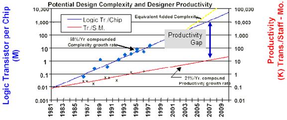
It is very clear that SystemVerilog is clearly targeted at improving designer productivity. Failing productivity due to increasing design complexity is one of the biggest challenges faced by chip designers today, and it is not at all surprising that the EDA tool industry is focused on rectifying this. The chart below (source: SEMATECH) shows a rather grim picture – while design complexity has been growing at 58% CAGR, productivity has been increasing at only 21% CAGR. It is obvious to anyone that tools that fill this gap will be in great demand.
Failing Designer Productivity (Source: SEMATECH)
The reason for increasing design complexity is multifold – decreasing geometries allow designers to add more and more elements to the chip, making the entire process challenging. Number of IP cores per chip has grown from ~30 in 2003 to over 250 in 2006 and possibly much more today (source: EETimes). In addition, a big bull’s eye has been painted on power consumption numbers and most chips now must be designed using low power techniques. Plus, increasing complexity means that chip verification becomes more complex; 50% of all ASIC designs today require respins due to functional/logic errors (Source: Colette International Research).
Rather than a single solution, it is very likely that a multitude of innovative solutions that address individual problems will emerge. For example, better modeling techniques that can give a very accurate QoR estimate at the architecture stage itself can reduce the design complexity downstream. Languages such as SystemVerilog literally reduce the lines of code that a designer or verification engineer must write, thus boosting productivity. Time also may be right for ESL design, which has been around for a while, as conventional techniques fail to keep up.
All in all, we live in very interesting times. Faster and smaller is not always for the better. The industry must innovate and rise up to the economic and design challenges if it is to survive and prosper.
What: Talk by Cliff Cummings on SystemVerilog FSM, Assertion, & RTL Tricks for Design Engineers When: Thursday, 5th November, 6:30pm to 8:00pm Where: Venture Center, NCL Innovation Park, Pashan Road. To reach Venture Center, go past NCL towards Pashan, pass the cricket ground adjacent to NCL and then you’ll find NCL Innovation Park / Venture Center on the right hand side. Map Registration and fees: This event is free for all to attend. No registration required.
Click on the image to see all PuneTech articles about PuneChips. Image via Wikipedia
SystemVerilog FSM, Assertion, & RTL Tricks for Design Engineers
Cliff Cummings is President of Sunburst Design, Inc., a company that specializes in world class Verilog, SystemVerilog and synthesis training. Mr. Cummings is an independent consultant and trainer with 27 years of ASIC, FPGA and system design experience and 17 years of Verilog, SystemVerilog, synthesis and methodology training experience. Mr. Cummings has completed many ASIC designs, FPGA designs and system simulation projects, and is capable of answering the very technical questions asked by experienced design engineers.
About PuneChips
PuneChips is a special interest group on semiconductor design and applications. PuneChips was formed to foster an environment for growth of companies in the semiconductor design and applications segment in the Pune area. Our goal is to build an ecosystem similar to PuneTech for companies in this field, where they can exchange information, consult with experts, and start and grow their businesses.
PuneChips has been started by Abhijit Athavale, president and CEO of Markonix, and a high-tech marketing consultant. He has 16+ years of high-technology industry experience. Prior to Markonix, Abhijit spent over 11 years at Xilinx, Inc. in various engineering, applications and marketing roles. In his role as a marketing consultant, he has held executive management positions at several companies. He has a masters degree in electrical engineering from Texas A&M University and a bachelors degree in electrical engineering from University of Pune. He is an accomplished speaker and author of several publications including a book.
Yesterday’s PuneTech post, “ASIC Verification: Trends and Challenges” was actually a guest post by Arati Halbe. Due to an oversight, I forgot to include the “About the Author” section in the post (in fact, I forgot to include any mention of the fact that the post was by Arati.) I apologize for the oversight.
(This is a guest post for PuneTech by Arati Halbe, who has close to 9 years experience in ASIC front end design and verification. Post silicon validation and FPGA prototyping is her recent area of interest and expertise. Arati has worked with Wipro Technologies and Conexant Systems. Arati did her B.E. from University of Pune and M.Tech from CEDT, Indian Institute of Science, Bangalore. See Arati’s linked-in profile for more details.)
As the complexity of Integrated Circuits (specifically ASIC and SoC) increases, and as their sizes keep reducing, the task of testing the chip gets more and more challenging. Engineers need to come up with better and different methodologies to ensure what goes to the factory for manufacturing is actually what they intended to deliver. Verification occurs at various stages in the ASIC development cycle. How much is enough at each stage is a problem that needs to be addressed on a case to case basis. A sound knowledge of various techniques and awareness of capabilities and limitations of each technique goes a long way in making decisions about when, where and what.
Click on the image to see all PuneChips articles on PuneTech. Image via Wikipedia
Keeping this in mind, PuneChips had verification expert Jagdish Doma talk about “ASIC verification: Trends and Challenges” on 20th August 2009. Though impacted by the H1N1 scare we had a small but diverse audience. Jagdish discussed in detail the strengths and limitations of the various techniques, viz: ESL, Formal verification, Dynamic simulation, FPGA prototyping and Emulation.
ESL or Electronic System Level testing is the newest trend. Supporters of ESL claim that it is a highly powerful system level modeling tool. It enables fast software bring-up if combined with an emulation/FPGA prototyping platform. ESL has been used successfully to validate systems for mobile applications where only one peripheral/application is active on the processor bus. ESL does not seem suitable for systems where multiple processes and interfaces are active simultaneously, like for example in a networking system.
Formal verification, a static verification technique which is mainly assertion based, is useful to check control paths. It cannot be used to verify datapaths. Dynamic simulation is a very effective way of verifying functionality of every block in the ASIC including the datapath. Gate level simulations performed after the back annotated placement and routing data is available are used to identify timing related issues or omissions/errors in stating multi-cycle paths.
The need to find hardware bugs as early as possible in the ASIC lifecycle drives the emulation and/or FPGA prototyping effort. Both these techniques enable the testing of scenarios which are generally not possible to test in dynamic functional verification, well before the actual silicon comes back from the fab. Emulation or prototyping also accelerate fast software ramp up and the software team can get a development platform ready well before the actual chip is available. Emulation involves running test cases on hardware accelerated platforms like Palladium from Cadence and Veloce from Mentor. For FPGA prototyping, Single or multiple FPGAs are used to build a PCB system targeted for the testing of the ASIC/SoC. The ASIC code is then fully or partially programmed on the FPGA/s and functionality can thus be tested.
Scenarios with much longer simulation times than what normal functional simulation allows can be run on the emulation platforms. All the internal signals are available for viewing and debug, just like in functional simulation. The FPGA prototype platform does enable longer test time, but the debugging available is limited. The hardware accelerators are costly, and investing in them makes sense if a company has lot of ASIC programs running simultaneously. For companies which have similar chips planned back to back, investing in a home grown FPGA based emulation/prototyping platform makes sense. Another advantage FPGA prototyping is that the RTL goes through a complete synthesis and place and route cycle and testing is done on a circuit which is as close to the real ASIC as possible.
To ensure that a bug free product reaches the customer is a complex activity and poses multiple challenges. Coverage, legacy code, repeatability are issues that need to be tackled. Ensuring that the coverage is at an acceptable level is important. Code coverage is run to find out if all the possibilities of a written code are exercised in a test suite. Simulators from cadence (ius), synopsys(vcs) and mentor (modelsim) have their own code coverage analyzers. Functional coverage means to find out if each feature listed in the specification for an ASIC/SoC is verified. It is essential that the functional specification document has an individual numbered paragraph for each feature so that traceability is easier. Functional coverage is an activity that needs planning, reviews and careful test case designing. Methodologies like eRM (e reuse methodology – Specman based) and OVM (open verification methodology – System verilog based) do assist checking functional coverage, but the inputs provided need careful specification and reviews.
Reviews, not just for coverage, but at every stage in the ASIC cycle are extremely important. One of the challenges encountered while designing an ASIC is that the hardware team interprets a certain behavior from software and the software expects that certain things are taken care of in hardware. It is very important to involve members from design team, verification team, architecture team, software & firmware team for verification review.
It takes a good amount of effort to come up with a verification environment, and it is very common for a team to use what has worked before when schedules are demanding. Legacy environment saves lot of time, but it also handicaps the team. Talking about saving time, efficiency goes a long way in shrinking the schedules. The initial time and effort investment in automation of repetitive tasks save lot of time in future. Use of re-usable methodologies will definitely save time and effort.
Finally, while choosing the verification flow for a certain ASIC, team needs to look at what is available in terms of resources as well as time, understand the end user requirement, and make a decision on which technique to employ at what stage.
What: Trends and Challenges by Jagdish Doma, former director of VLSI design for Conexant Systems When: Thursday, 20th August, 6:30pm to 8:00pm Where: Venture Center, NCL Innovation Park, Pashan Road. To reach Venture Center, go past NCL towards Pashan, pass the cricket ground adjacent to NCL and then you’ll find NCL Innovation Park / Venture Center on the right hand side. Map Registration and fees: This event is free for all to attend. No registration required.
Jagdish will discuss the ASIC verification flow, various verification and validation techniques, and strength areas and limitations of each technique and the key challenges faced by companies during the ASIC verification cycle.
About the speaker – Jagdish Doma
Jagdish served as Director of VLSI Division for Conexant Systems in Pune where he was responsible for managing diverse teams involved in design, verification, validation, implementation, physical design and software development. During his 19 year career, Jagdish has held various senoir techical positions at Texas Instruments, Cirrus Logic and AMD. He brings a wide range of experience in Architecture, Design, pre-silicon verification, post-silicon validation and leading organizations to successful product development. Jagdish holds Bachelor’s in Electrical Engineering from University of Pune and a Master’s in Electrical Engineering fromTexas A&M University.
About PuneChips
PuneChips is a special interest group on semiconductor design and applications. PuneChips was formed to foster an environment for growth of companies in the semiconductor design and applications segment in the Pune area. Our goal is to build an ecosystem similar to PuneTech for companies in this field, where they can exchange information, consult with experts, and start and grow their businesses.
PuneChips has been started by Abhijit Athavale, president and CEO of Markonix, and a high-tech marketing consultant. He has 16+ years of high-technology industry experience. Prior to Markonix, Abhijit spent over 11 years at Xilinx, Inc. in various engineering, applications and marketing roles. In his role as a marketing consultant, he has held executive management positions at several companies. He has a masters degree in electrical engineering from Texas A&M University and a bachelors degree in electrical engineering from University of Pune. He is an accomplished speaker and author of several publications including a book.
![Reblog this post [with Zemanta]](http://img.zemanta.com/reblog_b.png?x-id=728924c8-1dbe-416f-bf6b-cdbfb677d6f6)

![Reblog this post [with Zemanta]](http://img.zemanta.com/reblog_b.png?x-id=d4aa2e75-5a21-458e-9b7e-515596044b58)
![Reblog this post [with Zemanta]](http://img.zemanta.com/reblog_b.png?x-id=3c345993-e718-4033-9a19-55f231b7a203)
![Reblog this post [with Zemanta]](http://img.zemanta.com/reblog_b.png?x-id=7742b308-830f-4ef2-8c08-c59af36a6390)

![Reblog this post [with Zemanta]](http://img.zemanta.com/reblog_b.png?x-id=f4b9ba28-c4dd-46e1-aabe-80e0c4ff48a5)