Tag Archives: vlsi

Event: Impact of AI/ML on IoT

Fireside chat with CEO of Espressif, a fabless semiconductor company with presence in Shanghai, Pune, and Europe, which develops cutting-edge WiFi-and-Bluetooth enabled low-power IoT solutions, including the popular ESP8266 and ESP32 connected SoCs that are used by makers, startups and enterprises for building IoT/smart things. With over 100 million IoT chipsets sold and thousands of registered companies as customers, Espressif is at the cutting-edge of IoT product innovation and deployment.

This will be a conversation about Espressif’s journey to the platform it is today, challenges for a hardware startup, the current state of IoT, and how he sees artificial intelligence and machine learning driving IoT further. It should be a great opportunity for IoT enthusiasts, startups as well as hardware entrepreneurs.

Join us for a conversation with Espressif’s CEO & founder, Swee-Ann Teo from 6pm to 9pm, on Wednesday, 19th Dec. At Kirloskar Auditorium, Bhau Institute, COEP campus, Next to Boat Club

This event is open to free, and open to all. No registration required.

Opinion: Pune’s IT industry must focus on electronic design (ESDM) – Gouri Agtey Athale

Gouri Agtey Athale has an interesting article in the Pune Mirror pointing out that following the success of the “animation and gaming” niche sector, the IT industry in Pune should start focusing on other niche sectors – for example electronic design.

Excerpts:

[The] niche area of animation and gaming has worked out for Pune the way the software industry worked on the existing industrial base: combining the existing dormant and untapped potential and build a whole new business out of it.

Pune’s arrival on the animation and gaming scene has received recognition at the international level: two animation films made by companies based in Pune have made it to the list of Oscar nominations, Krayon’s Delhi Safari and Reliance Big’s Krishna and Kaunsa.

and

That was in the past: the move now is to move on and the next wave could be a convergence of the hardware and software sectors to create ESDM, or Electronic System Design and Manufacturing. Cmde (retd) Anand Khandekar, former member of the IT committee of the MCCIA, who helped draft the state’s IT policy over a decade ago, suggested that existing expertise in embedded software and the presence of the hardware sector in the city could be married to the city’s industrial culture and the educational base to create an industry around ESDM.

The blue print that ESDM is looking at is that of the automotive sector, where there are vendors who supply to the original equipment manufacturer, the OEM. On these lines, local entities could become vendors to global companies, the example usually cited being that of Taiwanbased companies who work on projects for global majors like Apple, Oracle-Sun Micro and Google- Motorola.

and finally:

And the sector needs a champion, a strong, non-partisan platform, which in the case of Pune’s software industry was the MCCIA.

Read the full article

Event Report: VLSI Design Conference Pune 2013

(This is an event report of the VLSI Design Conference that was held in Pune in Jan 2013, by Shakthi Kannan. It originally appeared on his blog, and is reproduced here with permission for the benefit of PuneTech readers.)

The 26th International Conference on VLSI Design 2013 and the 12th International Conference on Embedded Systems was held at the Hyatt Regency, Pune, India between January 5-10, 2013. The first two days were tutorial sessions, while the main conference began on Monday, January 7, 2013.
26th VLSID 2013

Day 1: Tutorial

On the first day, I attended the tutorial on “Concept to Product – Design, Verification & Test: A Tutorial” by Prof. Kewal Saluja, and Prof. Virendra Singh. Prof. Saluja started the tutorial with an introduction and history of VLSI. An overview of the VLSI realization process was given with an emphasis on synthesis. The theme of the conference was “green” technology, and hence the concepts of low power design were introduced. The challenges of multi-core and high performance design including cache coherence were elaborated. Prof. Singh explained the verification methodologies with an example of implementing a DVD player. Simulation and formal verification techniques were compared, with an overview on model checking. Prof. Saluja explained the basics of VLSI testing, differences between verification and testing, and the various testing techniques used. The challenges in VLSI testing were also discussed.

Day 2: Tutorial

On the second day, I attended the tutorial on “Formal Techniques for Hardware/Software Co-Verification” by Prof. Daniel Kroening, and Prof. Mandayam Srinivas. Prof. Kroening began the tutorial with the motivation for formal methods. Examples on SAT solvers, boundary model checking for hardware, and bounded program analysis for C programs were explained. Satisfiability modulo theories for bit-vectors, arrays and functions were illustrated with numerous examples. In the afternoon, Prof. Srinivas demoed formal verification for both Verilog and C. He shared the results of verification done for both a DSP and a microprocessor. The CProver tool has been released under a CMBC license. After discussion with Fedora Legal, and Prof. Kroening, it has been updated to a BSD license for inclusion in Fedora. The presentation slides used in the tutorial are available.

Day 3: Main conference

The first day of the main conference began with the keynote by Mr. Abhi Talwalker, CEO of LSI, on “Intelligent Silicon in the Data-centric Era”. He addressed the challenges in bridging the data deluge gap, latency issues in data centers, and energy efficient buildings. The second keynote of the day was given by Dr. Ruchir Puri, IBM Fellow, on “Opportunities and Challenges for High Performance Microprocessor Designs and Design Automation”. Dr. Ruchir spoke about the various IBM multi-core processors, and the challenges facing multi-core designs – software parallelism, socket bandwidth, power, and technology complexity. He also said that more EDA innovation needs to come at the system level.
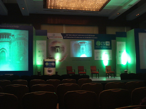
Dias

After the keynote, I attended the “C1. Embedded Architecture” track sessions. Liang Tang presented his paper on “Processor for Reconfigurable Baseband Modulation Mapping”. Dr. Swarnalatha Radhakrishnan then presented her paper on “A Study on Instruction-set Selection Using Multi-application Based Application Specific Instruction-Set Processors”. She explained about ASIPs (Application Specific Instruction Set Processor), and shared test results on choosing specific instruction sets based on the application domain. The final paper for the session was presented by Prof. Niraj K. Jha on “Localized Heating for Building Energy Efficiency”. He and his team at Princeton have used ultrasonic sensors to implement localized heating. A similar approach is planned for lighting as well.

Post-lunch, I attended the sessions for the track “B2. Test Cost Reduction and Safety”. The honourable chief minister of Maharashtra, Shri. Prithviraj Chavan, arrived in the afternoon to formally inaugurate the conference. He is an engineer who graduated from the University of California, Berkeley, and said that he was committed to put Pune on the semiconductor map. The afternoon keynote was given by Mr. Kishore Manghnani from Marvell, on “Semiconductors in Smart Energy Products”. He primarily discussed about LEDs, and their applications. This was followed by a panel discussion on “Low power design”. There was an emphasis to create system level, software architecture techniques to increase leverage in low power design. For the last track of the day, I attended the sessions on “C3. Design and Synthesis of Reversible Logic”. The Keccak sponge function family has been chosen to become the SHA-3 standard.

Day 4: Main conference

The second day of the main conference began with a recorded keynote by Dr. Paramesh Gopi, AppliedMicro, on “Cloud computing needs at less power and low cost” followed by a talk by Mr. Amal Bommireddy, AppliedMicro, on “Challenges of First pass Silicon”. Mr. Bommireddy discussed the factors affecting first pass success – RTL verification, IP verification, physical design, routing strategies, package design, and validation board design. The second keynote of the day was by Dr. Louis Scheffer from the Howard Hughes Medical Institute, on “Deciphering the brain, cousin to the chip”. It was a brilliant talk on applying chip debugging techniques to inspect and analyse how the brain works.

After the keynote, I visited the exhibition hall where companies had their products displayed in their respective stalls. AppliedMicro had a demo of their X-gene ARM64 platform running Ubuntu. They did mention to me that Fedora runs on their platform. Marvell had demonstrated their embedded and control solutions running on Fedora. ARM had their mbed.org and embeddedacademic.com kits on display for students. Post-lunch, was an excellent keynote by Dr. Vivek Singh, Intel Fellow, titled “Duniyaa Maange Moore!”. He started with what people need – access, connectivity, education, and healthcare, and went to discuss the next in line for Intel’s manufacturing process. The 14nm technology is scheduled to be operational by end of 2013, while 10nm is planned for 2015. They have also started work on 7nm manufacturing processes. This was followed by a panel discussion on “Expectations of Manufacturing Sector from Semiconductor and Embedded System Companies” where the need to bridge the knowledge gap between mechanical and VLSI/embedded engineers was emphasized.

Day 5: Main conference

The final day of the main conference began with the keynote by Dr. Vijaykrishnan Narayanan on “Embedded Vision Systems”, where he showed the current research in intelligent cameras, augmented reality, and interactive systems. I attended the sessions for the track “C7. Advances in Functional Verification”, and “C8. Logic Synthesis and Design”. Post-lunch, Dr. Ken Chang gave his keynote on “Advancing High Performance System-on-Package via Heterogeneous 3-D Integration”. He said that Intel’s 22nm Ivy Bridge which uses FinFETs took nearly 15 years to productize, but look promising for the future. Co(CoS) Chip on Chip on Substrate, and (CoW)oS Chip on Wafer on Substrate technologies were illustrated. Many hardware design houses use 15 FPGAs on a board for testing. The Xilinx Virtex-7HT FPGA has analog, memory, and ARM microprocessor integrated on a single chip giving a throughput of 2.8 Terabits/second. He also mentioned that Known Good Die (KGD) methodologies are still emerging in the market. For the last track of the conference, I attended the sessions on “C9. Advances in Circuit Simulation, Analysis and Design”.

Shakthi Kannan

Thanks to Red Hat for sponsoring me to attend the conference.

About the Author – Shakthi Kannan

Shakthi Kannan is a Senior Software Engineer with Red Hat in Pune, and is also a very active member of the open source community. For more details about him, see his Linkedin Profile, or his blog.

LiveBlog: Maharashtra CM Prithviraj Chavan’s address at VLSI Conf Pune

(This is a live-blog of the keynote address of Prithviraj Chavan, CM of Maharashtra, at the 26th International Conference on VLSI Design that is currently going on at the Hyatt, in Pune. For those who didn’t know, Prithviraj Chavan is an electrical engineer from BITS Pilani and Univ of California, Berkeley.)

The semiconductor industry in India started first in Bangalore, and then in Delhi/NCR. Pune is late to this game. But we have the potential to better than Delhi/NCR, and even Bangalore.

These are the things that need to happen for Pune to become a semiconductor hub:

  • Government should create facilities where the expensive EDA tools are setup, and various companies from industry can sign up for use of the tools.
  • Work on increasing the quality of manpower in and around Pune. We have to potential of having one of the highest ratios of high quality – low cost manpower. We need to work with universities and other educational institutions in this area.
  • We should continue trying to attract fabs to come and setup in Pune

We are a large customer of mobiles and other electronic devices. As we continue to grow at 8-9%, we will become an increasingly attractive market. And there will also be many opportunities to create specialized devices for local markets. This can drive innovation and incubation.

The CM said that he is completely committed to working with us (i.e. the tech community in Pune) to ensure that Pune gets put on the semiconductor map. He announced that any company investing in semiconductors in Maharashtra will get a rebate on their VAT until they recoup their investment. In addition, he hopes that the government will be able to help jumpstart this industry by these means:

  • Government will set up the physical infrastructure
  • Government will put up the initial funding for the expensive tools
  • Government will set up training facilities to get people started on this
  • We should together set up server farms, and other infrastructure needed to get started

Maharashtra is larger than most countries in the world, as large as Mexico, and larger than any European country. It attracts 33% of the FDI that came into the country. Maharashtra is well positioned to become the chip destination of India.

#VLSI-Conf-Pune 2013 Event Report: Intelligent Silicon in the Data-Centric Era

(This is a live-blog of the keynote address given by Abhi Talwalkar at the 26th International Conference on VLSI Design being held in Pune. Abhi is the President and CEO of LSI Corporation. (LSI has had a large development center in Pune for the last 4 years.)

(Note: since this is a live-blog, it is only a partial and unorganized report, and might contain errors and omissions.)

The innovation happening in the world since the first transistor was developed has been unparalleled in history. This has led to various changes, including a flat world where anyone can innovate from anywhere in the world, there is lots and lots of collaboration, and where for the first time, information and data are the most important currency.

As a result, we are now seeing a deluge of data. The reasons are:

  • Everybody is on social networks and creating/sharing data
  • Everyone has personal devices (8.5 billion devices sold per year, 40% of them are smart devices), and again people are living a lot of their lives through these devices
  • Other devices are generating data automatically, and will continue to do so

The technology challenges resulting from this data deluge are in the areas of devices, the data centers and the network. These are the challenges in these areas:

  • Bring your own device. Previously, companies insisted on employees using company approved devices (e.g. Blackberry only, and no iPhones). But more and more employees want to use their own devices, and company IT departments are forced to deal with them. The variety of devices that need to be supported is a proble. And the devices need to be always on and always connected – and so do the enterprise backend apps that need to support these devices. The enterprise IT apps need to support mobile devices seamlessly, and in general there is a consumerization of enterprise IT – driving a newfound focus on improved end-user experiences.
  • Green Impact of Devices: All these devices generate e-waste, emissions and use up energy
  • Network bottlenecks: the wireless spectrum which these devices use is getting congested. The backhaul network connections are also facing a capacity crunch. And security in all these areas is an area of increasing concern.
  • Green Impact of DataCenters: Data centers have increased energy consumption by 3x. Telecom in India consumes 3 billion litres of diesel. This is second only to railways, and is a major contributor to the carbon emissions.

Since most of the above seem like software challenges, what does Silicon (Hardware/VLSI/Embedded systems) have to do with them? The answer is that silicon allows you do more with less, and is a key catalyst for innovation. There is much more power in CPUs today than we need – and we need to figure out how to use it. There needs to be more intelligent hardware which knows how to protect the data, where to move it, etc.

What are the specific problems that can/should be solved in silicon?

  • Hardware Accelerators: A full suite of silicon based accelerators can be deployed in the network and the data center.
  • Improve latency and capacity: utilization levels continue to remain low in data-centers, and can be improved significantly
  • Intelligent caching: For example, appropriate use of flash memory between magnetic storage and memory can get much better performance without a significant increase in infrastructure.
  • Use sensors and gather data to make the silicon more intelligent and take better decisions. For example, many companies would leave lights on all night but now more and more are deploying sensors which will turn off the lights when not required. This concept can be extended to many other areas.

PuneChips Event: Building an Autonomous and Scalable Semiconductor VLSI Business

PuneChips, the forum for everybody interested VLSI, semiconductor and embedded technologies in Pune, along with LSI Corporation invite you to a talk on Building an Autonomous and Scalable Semiconductor VLSI Business. This talk is by Dr. T.R. Ramachandra, a Senior Director in the Storage Peripherals division of LSI.

The talk is on Wednesdah, 13 July, from 9:30am to 11am at LSI’s office near the airport.

Abstract: Building an Autonomous and Scalable Semiconductor VLSI Business

The presentation focuses on effective ways to build autonomous and scalable semiconductor VLSI businesses. The trends in the VLSI industry and inherent challenges of growth make autonomy & scale-building essential elements of long-term success. This is particularly relevant to emerging geographies like India where there is increased focus on enhancing end-to-end capabilities and overall management.

About the Speaker – Dr. T.R. Ramachandran

T. R. Ramachandran is Senior Director for Product Operations in the Storage Peripherals Division at LSI. In this role, he reports to the Senior Vice President and General Manager of the division and is responsible for the operations infrastructure, business processes, IP and customer program management across the entire product lifecycle from planning through manufacturing ramp for LSI’s highest volume semiconductor business. Before assuming this role, TR held a number of positions in LSI where he brought to bear a unique blend of expertise in a range of areas from business, operations & program management, strategic/competitive analysis, large-scale M&A and business transformations, global product development and deployment, and supplier & manufacturing management. He lives in the United States in Northern California, and is keenly interested in various aspects of technology & broader public policy as well as problems of scale tied to private, public and/or non-governmental sectors.

TR received a Bachelor’s degree in Metallurgical Engineering from IIT-M (Indian Institute of Technology in Madras/Chennai) and is a recipient of the Dr. Dhandapani Prize from IIT-M and the Vidya Bharati Prize conferred by the Indian Institute of Metals. He received his Masters and Ph.D. degrees in Materials Science from the University of Southern California, Los Angeles. His Ph.D. was focused on structural and optical studies of semiconductor thin films & quantum dot nanostructures and innovative forays into nanotechnology using scanning probe microscopes.

About Pune Chips

PuneChips is a special interest group on semiconductor design and applications. PuneChips was formed to foster an environment for growth of companies in the semiconductor design and applications segment in the Pune area. Our goal is to build an ecosystem similar to PuneTech for companies in this field, where they can exchange information, consult with experts, and start and grow their businesses.

For more information, see the PuneChips website, and/or join the PuneChips mailing list. Please forward to anybody in Pune who is interested in renewable energy, solar technologies, semiconductors, chip design, VLSI design, chip testing, and embedded applications.

Fees and registration

This event is free and open for anybody to attend. RSVP Reshma Arthani: Reshma.Artani@lsi.com, Mobile: +91.992.320.3557

The talk is at: Sargam Auditorium, 4th floor, LSI India, Commerzone, Samrat Ashok Path, Off Airport Road. Wednesday 13 July, 9:30am.

PuneChips Event: Advanced System Verilog Tips with Cliff Cummings – 19th April

Abhijit Athavale writes:

SystemVerilog Guru Cliff Cummings is back in town and he will be holding another seminar on April 19th at MCCIA’s Sumant Moolgaokar Auditorium, ICC Towers, Senapati Bapat Road from 4:00pm to 7:30pm. Most recently, Cliff was here in November 2009 and this seminar gives a great opportunity for engineers to re-engage with him.

The topics covered will include:

  • New UVM 1.0 overview and comparison to OVM
  • Important OVM and UVM phasing
  • Secrets in mastering OVM and UVM
  • Graceful termination of tests in OVM and UVM with emphasis on the objection mechanism
  • Some of Cliff’s favorite SystemVerilog tips and tricks
  • Some early UVM techniques and best practices

This event is co-sponsored by Qlogic and Cadence who I must thank profusely on behalf of the PuneChips community. It is not very often that internationally renowned experts visit our city and hold free seminars, but QLogic and Cadence have made it possible. So, I encourage everyone who has any interest in SystemVerilog to attend and participate.

This event is completely free, but registration is required. Please visit this link to register and view the agenda.

Materials, mechanics, thermals, speed, power – Overview of Integrated Circuit Packaging – PuneChips 10th July

What: Overview of the field of electronics packaging – by Dr. Sandeep Sane, Intel Corp, (Ph.D. CalTech)
When: Saturday, 10 July, 10:30am to 12:30pm
Where: Venture Center, NCL Innovation Park, Pashan Road. To reach Venture Center, go past NCL towards Pashan, pass the cricket ground adjacent to NCL and then you’ll find NCL Innovation Park / Venture Center on the right hand side. Map
Registration and fees: This event is free for all to attend. No registration required.

PuneChips is a PuneTech special interest group on semiconductors, VLSI, embedded, and EDA. Click on the Logo to see all PuneTech articles about PuneChips

Electronic Packaging – Materials and Mechanics Challenges

Electronic packaging has typically been defined as providing an enabling function and a space transformer between the IC feature sizes and the board & system level interconnects and over years it has grown to become a ubiquitous part of the overall electronic assembly. In certain market segments, such as flash memories, the package has evolved to become a key product differentiator and performance enabler. The scope of electronic packaging is very broad across multiple application areas such as CPUâs and Chipsets for the desktop, mobile and server segments, hand-held and wireless devices, telecom components & network processors, and memory devices; with each segment potentially having its unique set of demands and constraints such as the form factor, function, cost, reliability requirements, thermal and electrical performance.

To ensure that right technical and cost-effective solutions are defined, developed and deployed across the different market segments, electronic packaging provides significant research and development challenges and opportunities across multiple disciplines including materials, mechanics, reliability, thermals, high speed interconnects, power delivery and manufacturing.

This presentation will first provide an overview of current and future package technologies and associated demands in the different market segments, followed by focusing on some of the recent progress made in addressing some of the mechanics and materials challenges and highlight opportunities in future packaging technology development.

About the speaker – Dr. Sandeep Sane

Sandeep Sane received his Ph.D. from California Institute of Technology, Pasadena in Aerospace Engineering with major in Solid Mechanics. He holds M.S. in Aeronautics, California Institute of Technology and B.Tech in Mechanical Engineering from Indian Institute of Technology, Bombay (Mumbai).

Sandeep is currently a Technology Development manager in the Assembly and Test Technology Development (ATTD) organization, Intel Corp., Chandler. He manages a technical team of 30 engineers including an experimental mechanics laboratory; equipped with start of art analysis and validation metrologies. His team is chartered to deliver fundamental understanding of various mechanical issues in electronic packaging, establish roadmaps for ATTD and work directly with Intelâs customers (OEM/ODMs) and suppliers to resolve mechanical issues. He is also responsible for delivering novel mechanical analysis, material characterization and validation techniques to help optimize design, material and process changes to deliver reliable and cost effective solutions for Intelâs packaging technologies. Sandeep has led and participated in numerous taskforces and management review boards to resolve critical issues in a timely manner impacting Intelâs bottom-line. Prior to joining Intel, he was a Development Staff Engineer with IBM, Endicott, NY, working in Mechanical & Thermal Analysis group.

Sandeep has filed for more than 15 patents and have published several technical articles in various conferences and journal proceedings. He is also a recipient of numerous awards across Intel for his technical contributions. He is a member of ASME, IEEE and an active member of organizing committees for ASME and IEEE conferences. He also serves on Industrial Advisory Board for Mechanical Engineering at University of Colorado, Boulder and NSF review committee.

About Venture Center

Entrepreneurship Development Center (Venture Center) – a CSIR initiative – is a not-for-profit company hosted by the National Chemical Laboratory, Pune. Venture Center strives to nucleate and nurture technology and knowledge-based enterprises by leveraging the scientific and engineering competencies of the institutions in the Pune region in India. The Venture Center is a technology business incubator specializing in technology enterprises offering products and services exploiting scientific expertise in the areas of materials, chemicals and biological sciences & engineering.

About PuneChips

PuneChips is a special interest group on semiconductor design and applications. PuneChips was formed to foster an environment for growth of companies in the semiconductor design and applications segment in the Pune area. Our goal is to build an ecosystem similar to PuneTech for companies in this field, where they can exchange information, consult with experts, and start and grow their businesses.

PuneChips has been started by Abhijit Athavale, president and CEO of Markonix, and a high-tech marketing consultant. He has 16+ years of high-technology industry experience. Prior to Markonix, Abhijit spent over 11 years at Xilinx, Inc. in various engineering, applications and marketing roles. In his role as a marketing consultant, he has held executive management positions at several companies. He has a masters degree in electrical engineering from Texas A&M University and a bachelors degree in electrical engineering from University of Pune. He is an accomplished speaker and author of several publications including a book.

For more information, see the PuneTech wiki profile of PuneChips, and/or join the PuneChips mailing list.

Please forward this mail to anybody in Pune who is interested in semiconductors, chip design, VLSI design, chip testing, and embedded applications.

Introducing http://PuneChips.com: The PuneTech SIG on Semiconductors, EDA, VLSI, Embedded Systems

Over the past 2 years, PuneTech has covered a breadth of technology related topics, with a concentration on Information Technology & Software. The strategic goal is to cover multiple technology segments and discuss innovative & exciting developments in these areas; specifically in Pune’s context.

It was with this objective that the concept of ‘SIG’ (Special Interest Group) was first mooted last year. A SIG covers a given vertical or horizontal domain area in depth. We decided that the best way to expand PuneTech would be to create a number of such SIGs, each focused on some particular vertical, and each run by someone who is passionate about that vertical. PuneTech would provide support, like a launching pad, publicity and visibility, and guidance about what works and what doesn’t work, based on our own experiences. Over time, we expect SIGs to have their own websites, and their own offline events.

PuneChips is a PuneTech special interest group on semiconductors, VLSI, embedded, and EDA. Click on the Logo to see all PuneTech articles about PuneChips

PuneChips was the first SIG, launched in June of 2009, launched by Abhijit Athavale (SIG Leader) in cooperation with PuneTech. It focuses on semiconductors design and applications. This SIG has arranged many successful meetings and events, and now it has also launched has its own website: www.punechips.com . This website features information about the PuneChips events, as well as blogs about the semiconductors and embedded system industry. Volunteers like Arati Halbe have helped with PuneChips (but more volunteers are needed). Also, the Venture Center and Kaushik Gala have been helpful in graciously providing their premises for holding PuneChips events. For more details see the PuneChips about page.

PuneTech hopes to incubate more SIGs like PuneChips in future, and spin them off as separate entities. PuneTech will continue to be actively involved in supporting and publicizing the events and activities of these SIGs. If you’d like to start one, please get in touch with us.

PuneChips Activities

Over the past 8 months, PuneChips has organized a number of interesting meetings, featuring senior thought leaders from the semiconductor industry. It also has an active google-groups mailing list and a ‘Pune Chips’ linkedin group. Nearly 200 professionals and students from the VLSI, Embedded Systems, and other related areas are members of these groups. You can also follow PuneChips on twitter.

The first kick-off meeting of PuneChips in June 2009 featured Abhijit Abhyankar, Head of Rambus India. His talk on Emerging opportunities in the semiconductor industry presented a nice overview of the semiconductor sector and its progression over the past few decades. He also discussed emerging opportunities and trends in this field.

The second event featured Shrinath Keskar, ex-MD of Ikanos India. His presentation: IC Design Challenges in the Telecom sector discussed the various challenges in IC Design, specifically with respect to the Telecom Sector.

The August 2009 speaker Jagdish Doma, former director of VLSI design Conexant Systems, covered ASIC Verification trends and challenges.

The October 2009 session featured a talk by Cliff Cummings, President of Sunburst Design and SystemVerilog Industry Guru. He talked about SystemVerilog & Designer Productivity, discussing specific tools and tricks for improving designer productivity.

The January session featured Madhu Atre, President of Applied Materials India. His talk on A Bright Solar Future discussed the various new developments in the area of solar power (specifically photo-voltaic) and the macro alternate energy global trends. He also touched upon the implications of these developments for India, including costs and government incentives.

In 2010, PuneChips plans to arrange similar meetings, featuring talks by thought leaders from the industry. The SIG also looks forward to more active interactions on the mailing list and linkedin group. If you are interested in learning more about the PuneChips activities and/or have a speaker you would like to recommend, please contact Abhijit Athavale.

You should form a SIG too – Get in touch with us

It would be great if Pune has many more such SIGs. A number of such groups and organizations are already active (some like the Pune Linux Users Group have existed long before PuneTech was started, and most like the Pune Open Coffee Club, for entrepreneurs and startups, were created independently). But there is scope for many more. The existing ones largely tend to be focused on particular technologies (like the Google Technologies User Group, or the Pune User Group for Microsoft Technologies). There are only a few that are aligned with industry verticals, like PuneChips or the Null group focused on security. I think there should be more.
So, if you’re passionate about some industry vertical, and are willing to spend at least a few hours a week on organizing a Pune-based SIG around that vertical, and are willing to do that for at least a couple of years, please let in touch with us, and let us make it happen.

In fact, it does not even have to be a vertical. It can be a horizontal area that goes across groups. As long as it is something that benefits Pune’s techies, we are game. In fact, we’re soon expecting to make an announcement related to PuneTech and Marathi. Subscribe to PuneTech so you don’t miss it.

PuneChips event: Wavelet Transform & its Applications in Image Processing – 6th March

(This article about a PuneChips event is reproduced with permission from the PuneChips website)

What: Talk by Ganesh Bhokare on Wavelet Transform & its Applications in Image Processing
When
: Saturday, 6th March 2010, 10:00 am to 12:00 noon.
Where: Venture Center, NCL Innovation Park, Pashan Road
Registration and fees: This event is *FREE* for all to attend. No registration required.

PuneChips is a PuneTech special interest group on semiconductors, VLSI, embedded, and EDA. Click on the image to see all PuneTech articles about PuneChips
An image of a two level wavelet transform. A PuneChips event, on the Wavelet Transform and its applications in Image Processing will be held in Venture Center on 6th March. PuneChips is a PuneTech special interest group on semiconductors, VLSI, embedded, and EDA. Click on the Logo to see all PuneTech articles about PuneChips. Image by Alessio Damato via Wikipedia.

Wavelet Transform & its Applications in Image Processing

In today’s multimedia wireless communication , major issue is bandwidth needed to satisfy real time transmission of audio and video data. The solution to this problem is to efficiently compress audio and video data for a given SNR. Wavelet transform is an evolving technology which offers far higher degrees of data compression compared to standard transforms such as DCT etc. In this talk we will be discussing concepts of wavelet transform and its applications to image compression and processing. The same can be extended to video processing.

About the speaker – Ganesh Bhokare

Ganesh Bhokare has over 15 years experience in using DSP audio, video and Embedded systems for Digital Media Processing. He is a PhD candidate at IIT Mumbai and currently in the process of defending his thesis. He has professional experience with  NXP, Conexant, TI and Cirrus Logic.

About Venture Center

Entrepreneurship Development Center (Venture Center) – a CSIR initiative – is a not-for-profit company hosted by the National Chemical Laboratory, Pune. Venture Center strives to nucleate and nurture technology and knowledge-based enterprises by leveraging the scientific and engineering competencies of the institutions in the Pune region in India. The Venture Center is a technology business incubator specializing in technology enterprises offering products and services exploiting scientific expertise in the areas of materials, chemicals and biological sciences & engineering.

About PuneChips

PuneChips is a special interest group on semiconductor design and applications. PuneChips was formed to foster an environment for growth of companies in the semiconductor design and applications segment in the Pune area. Our goal is to build an ecosystem similar to PuneTech for companies in this field, where they can exchange information, consult with experts, and start and grow their businesses.

For more information, see the PuneChips website at http://punechips.com, and/or join the PuneChips mailing list: http://groups.google.com/group/punechips.  Please forward this mail to anybody in Pune who is interested in renewable energy, solar technologies, semiconductors, chip design, VLSI design, chip testing, and embedded applications.

Reblog this post [with Zemanta]

Comments are closed on this article. Please comment at the original article