Tag Archives: embedded

Event Report: VLSI Design Conference Pune 2013

(This is an event report of the VLSI Design Conference that was held in Pune in Jan 2013, by Shakthi Kannan. It originally appeared on his blog, and is reproduced here with permission for the benefit of PuneTech readers.)

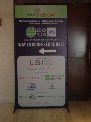
The 26th International Conference on VLSI Design 2013 and the 12th International Conference on Embedded Systems was held at the Hyatt Regency, Pune, India between January 5-10, 2013. The first two days were tutorial sessions, while the main conference began on Monday, January 7, 2013.

26th VLSID 2013

Day 1: Tutorial

On the first day, I attended the tutorial on “Concept to Product – Design, Verification & Test: A Tutorial” by Prof. Kewal Saluja, and Prof. Virendra Singh. Prof. Saluja started the tutorial with an introduction and history of VLSI. An overview of the VLSI realization process was given with an emphasis on synthesis. The theme of the conference was “green” technology, and hence the concepts of low power design were introduced. The challenges of multi-core and high performance design including cache coherence were elaborated. Prof. Singh explained the verification methodologies with an example of implementing a DVD player. Simulation and formal verification techniques were compared, with an overview on model checking. Prof. Saluja explained the basics of VLSI testing, differences between verification and testing, and the various testing techniques used. The challenges in VLSI testing were also discussed.

Day 2: Tutorial

On the second day, I attended the tutorial on “Formal Techniques for Hardware/Software Co-Verification” by Prof. Daniel Kroening, and Prof. Mandayam Srinivas. Prof. Kroening began the tutorial with the motivation for formal methods. Examples on SAT solvers, boundary model checking for hardware, and bounded program analysis for C programs were explained. Satisfiability modulo theories for bit-vectors, arrays and functions were illustrated with numerous examples. In the afternoon, Prof. Srinivas demoed formal verification for both Verilog and C. He shared the results of verification done for both a DSP and a microprocessor. The CProver tool has been released under a CMBC license. After discussion with Fedora Legal, and Prof. Kroening, it has been updated to a BSD license for inclusion in Fedora. The presentation slides used in the tutorial are available.

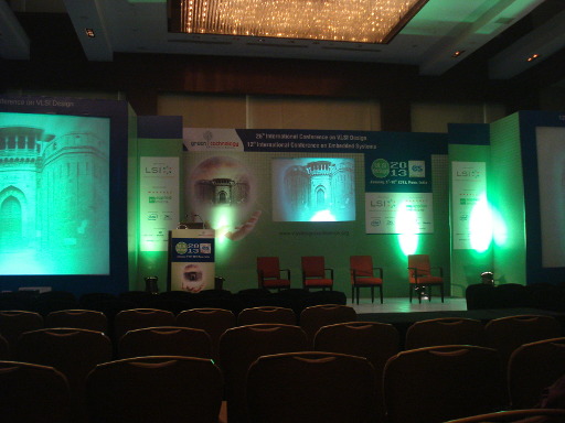
Day 3: Main conference

The first day of the main conference began with the keynote by Mr. Abhi Talwalker, CEO of LSI, on “Intelligent Silicon in the Data-centric Era”. He addressed the challenges in bridging the data deluge gap, latency issues in data centers, and energy efficient buildings. The second keynote of the day was given by Dr. Ruchir Puri, IBM Fellow, on “Opportunities and Challenges for High Performance Microprocessor Designs and Design Automation”. Dr. Ruchir spoke about the various IBM multi-core processors, and the challenges facing multi-core designs – software parallelism, socket bandwidth, power, and technology complexity. He also said that more EDA innovation needs to come at the system level.

Dias

After the keynote, I attended the “C1. Embedded Architecture” track sessions. Liang Tang presented his paper on “Processor for Reconfigurable Baseband Modulation Mapping”. Dr. Swarnalatha Radhakrishnan then presented her paper on “A Study on Instruction-set Selection Using Multi-application Based Application Specific Instruction-Set Processors”. She explained about ASIPs (Application Specific Instruction Set Processor), and shared test results on choosing specific instruction sets based on the application domain. The final paper for the session was presented by Prof. Niraj K. Jha on “Localized Heating for Building Energy Efficiency”. He and his team at Princeton have used ultrasonic sensors to implement localized heating. A similar approach is planned for lighting as well.

Post-lunch, I attended the sessions for the track “B2. Test Cost Reduction and Safety”. The honourable chief minister of Maharashtra, Shri. Prithviraj Chavan, arrived in the afternoon to formally inaugurate the conference. He is an engineer who graduated from the University of California, Berkeley, and said that he was committed to put Pune on the semiconductor map. The afternoon keynote was given by Mr. Kishore Manghnani from Marvell, on “Semiconductors in Smart Energy Products”. He primarily discussed about LEDs, and their applications. This was followed by a panel discussion on “Low power design”. There was an emphasis to create system level, software architecture techniques to increase leverage in low power design. For the last track of the day, I attended the sessions on “C3. Design and Synthesis of Reversible Logic”. The Keccak sponge function family has been chosen to become the SHA-3 standard.

Day 4: Main conference

The second day of the main conference began with a recorded keynote by Dr. Paramesh Gopi, AppliedMicro, on “Cloud computing needs at less power and low cost” followed by a talk by Mr. Amal Bommireddy, AppliedMicro, on “Challenges of First pass Silicon”. Mr. Bommireddy discussed the factors affecting first pass success – RTL verification, IP verification, physical design, routing strategies, package design, and validation board design. The second keynote of the day was by Dr. Louis Scheffer from the Howard Hughes Medical Institute, on “Deciphering the brain, cousin to the chip”. It was a brilliant talk on applying chip debugging techniques to inspect and analyse how the brain works.

After the keynote, I visited the exhibition hall where companies had their products displayed in their respective stalls. AppliedMicro had a demo of their X-gene ARM64 platform running Ubuntu. They did mention to me that Fedora runs on their platform. Marvell had demonstrated their embedded and control solutions running on Fedora. ARM had their mbed.org and embeddedacademic.com kits on display for students. Post-lunch, was an excellent keynote by Dr. Vivek Singh, Intel Fellow, titled “Duniyaa Maange Moore!”. He started with what people need – access, connectivity, education, and healthcare, and went to discuss the next in line for Intel’s manufacturing process. The 14nm technology is scheduled to be operational by end of 2013, while 10nm is planned for 2015. They have also started work on 7nm manufacturing processes. This was followed by a panel discussion on “Expectations of Manufacturing Sector from Semiconductor and Embedded System Companies” where the need to bridge the knowledge gap between mechanical and VLSI/embedded engineers was emphasized.

Day 5: Main conference

The final day of the main conference began with the keynote by Dr. Vijaykrishnan Narayanan on “Embedded Vision Systems”, where he showed the current research in intelligent cameras, augmented reality, and interactive systems. I attended the sessions for the track “C7. Advances in Functional Verification”, and “C8. Logic Synthesis and Design”. Post-lunch, Dr. Ken Chang gave his keynote on “Advancing High Performance System-on-Package via Heterogeneous 3-D Integration”. He said that Intel’s 22nm Ivy Bridge which uses FinFETs took nearly 15 years to productize, but look promising for the future. Co(CoS) Chip on Chip on Substrate, and (CoW)oS Chip on Wafer on Substrate technologies were illustrated. Many hardware design houses use 15 FPGAs on a board for testing. The Xilinx Virtex-7HT FPGA has analog, memory, and ARM microprocessor integrated on a single chip giving a throughput of 2.8 Terabits/second. He also mentioned that Known Good Die (KGD) methodologies are still emerging in the market. For the last track of the conference, I attended the sessions on “C9. Advances in Circuit Simulation, Analysis and Design”.

Shakthi Kannan

Thanks to Red Hat for sponsoring me to attend the conference.

About the Author – Shakthi Kannan

Shakthi Kannan is a Senior Software Engineer with Red Hat in Pune, and is also a very active member of the open source community. For more details about him, see his Linkedin Profile, or his blog.

LiveBlog: Maharashtra CM Prithviraj Chavan’s address at VLSI Conf Pune

(This is a live-blog of the keynote address of Prithviraj Chavan, CM of Maharashtra, at the 26th International Conference on VLSI Design that is currently going on at the Hyatt, in Pune. For those who didn’t know, Prithviraj Chavan is an electrical engineer from BITS Pilani and Univ of California, Berkeley.)

The semiconductor industry in India started first in Bangalore, and then in Delhi/NCR. Pune is late to this game. But we have the potential to better than Delhi/NCR, and even Bangalore.

These are the things that need to happen for Pune to become a semiconductor hub:

  • Government should create facilities where the expensive EDA tools are setup, and various companies from industry can sign up for use of the tools.
  • Work on increasing the quality of manpower in and around Pune. We have to potential of having one of the highest ratios of high quality – low cost manpower. We need to work with universities and other educational institutions in this area.
  • We should continue trying to attract fabs to come and setup in Pune

We are a large customer of mobiles and other electronic devices. As we continue to grow at 8-9%, we will become an increasingly attractive market. And there will also be many opportunities to create specialized devices for local markets. This can drive innovation and incubation.

The CM said that he is completely committed to working with us (i.e. the tech community in Pune) to ensure that Pune gets put on the semiconductor map. He announced that any company investing in semiconductors in Maharashtra will get a rebate on their VAT until they recoup their investment. In addition, he hopes that the government will be able to help jumpstart this industry by these means:

  • Government will set up the physical infrastructure
  • Government will put up the initial funding for the expensive tools
  • Government will set up training facilities to get people started on this
  • We should together set up server farms, and other infrastructure needed to get started

Maharashtra is larger than most countries in the world, as large as Mexico, and larger than any European country. It attracts 33% of the FDI that came into the country. Maharashtra is well positioned to become the chip destination of India.

#VLSI-Conf-Pune 2013 Event Report: Intelligent Silicon in the Data-Centric Era

(This is a live-blog of the keynote address given by Abhi Talwalkar at the 26th International Conference on VLSI Design being held in Pune. Abhi is the President and CEO of LSI Corporation. (LSI has had a large development center in Pune for the last 4 years.)

(Note: since this is a live-blog, it is only a partial and unorganized report, and might contain errors and omissions.)

The innovation happening in the world since the first transistor was developed has been unparalleled in history. This has led to various changes, including a flat world where anyone can innovate from anywhere in the world, there is lots and lots of collaboration, and where for the first time, information and data are the most important currency.

As a result, we are now seeing a deluge of data. The reasons are:

  • Everybody is on social networks and creating/sharing data
  • Everyone has personal devices (8.5 billion devices sold per year, 40% of them are smart devices), and again people are living a lot of their lives through these devices
  • Other devices are generating data automatically, and will continue to do so

The technology challenges resulting from this data deluge are in the areas of devices, the data centers and the network. These are the challenges in these areas:

  • Bring your own device. Previously, companies insisted on employees using company approved devices (e.g. Blackberry only, and no iPhones). But more and more employees want to use their own devices, and company IT departments are forced to deal with them. The variety of devices that need to be supported is a proble. And the devices need to be always on and always connected – and so do the enterprise backend apps that need to support these devices. The enterprise IT apps need to support mobile devices seamlessly, and in general there is a consumerization of enterprise IT – driving a newfound focus on improved end-user experiences.
  • Green Impact of Devices: All these devices generate e-waste, emissions and use up energy
  • Network bottlenecks: the wireless spectrum which these devices use is getting congested. The backhaul network connections are also facing a capacity crunch. And security in all these areas is an area of increasing concern.
  • Green Impact of DataCenters: Data centers have increased energy consumption by 3x. Telecom in India consumes 3 billion litres of diesel. This is second only to railways, and is a major contributor to the carbon emissions.

Since most of the above seem like software challenges, what does Silicon (Hardware/VLSI/Embedded systems) have to do with them? The answer is that silicon allows you do more with less, and is a key catalyst for innovation. There is much more power in CPUs today than we need – and we need to figure out how to use it. There needs to be more intelligent hardware which knows how to protect the data, where to move it, etc.

What are the specific problems that can/should be solved in silicon?

  • Hardware Accelerators: A full suite of silicon based accelerators can be deployed in the network and the data center.
  • Improve latency and capacity: utilization levels continue to remain low in data-centers, and can be improved significantly
  • Intelligent caching: For example, appropriate use of flash memory between magnetic storage and memory can get much better performance without a significant increase in infrastructure.
  • Use sensors and gather data to make the silicon more intelligent and take better decisions. For example, many companies would leave lights on all night but now more and more are deploying sensors which will turn off the lights when not required. This concept can be extended to many other areas.

Ajit Shelat, 1 Sept 2010

(Pune based serial entrepreneur, Ajit Shelat, passed away yesterday. This article and photo are by flickr user drona and are taken from this page. They’re reproduced here under the terms of the Creative Commons (BY-NC) license under which that page is published.)

Ajit Shelat

My friend Ajit Shelat passed away today. He was driving on the Mumbai-Pune Highway, and had an accident at about 530pm September 1, 2010.

He was a fellow alumnus and contemporary of IIT-Mumbai.

Trained entirely in India, he was perhaps the first Indian engineer who designed and developed a very complex LAN security chipset at Nevis Networks, entirely based out of Pune, India.

He was a co-founder of RIMO technologies, Switch-on Networks(with Moti Jiandani), and Nevis Networks. Switch-On Networks was sold to PMC-Sierra for $300M+.

He supported a wide variety of environmental causes and an avid hiker and naturalist. A prolific entrepreneur himself, he generously gave his time and money to his favorite causes: The environment, education and entrepreneurs.

Said Yatin Mundkur, a venture capitalist at Artiman Ventures, who used to work for Ajit at Godrej Industries, in the mid-eighties: “I am who I am today, because of Ajit. And a lot of us who reported to him at Godrej would gladly say that.”

I will fondly remember the many hikes I took with him, and particularly the many discussions I had with him during the early X Window System days.

He is survived by his wife Radha Shelat and daughter Arundhati, and mother and sister.

drona

(Ajit Shelat was most recently the President and CEO of Nevis Networks, a company that he was trying to turn around after he and his partners had acquired the assets of the company from the previous investors. PuneTech had interviewed Ajit just before this. He is survived by his wife, Radha Shelat, (VP Engineering, and India MD of Librato, previously CTO of Symantec Pune & Veritas Pune), and daughter.)

Enhanced by Zemanta

India/China better markets today for tech startups – Ajit Shelat, SVP, Nevis Networks

Ajit Shelat Nevis Networks
Ajit Shelat, Senior Vice President of Engineering, Nevis Networks

Nevis Networks, a mostly-Pune-based-company (with “official” headquarters in the US, and an additional center in China), builds network switches and other network hardware that allows a company to secure it’s internal network from attacks and to enforce identity-based security policies. The company’s LANenforcer product family transparently protects the network from external malicious attacks, and also allows restricting access to different network resources based on users’ identities according to policies set by the system administrators. This can be customized to ensure different levels of access to different classes of users, employees, contractors, guests and other third parties. In addition, the product allows detailed reporting, auditing, employee activity reports that make it possible to analyze security breaches in very granular detail. And because it is hardware based, all of this is delivered in realtime with very low latency.

Nevis Networks’ customers range from financial services, healthcare, education and defense contractors and they deploy Nevis LANenforcers to protect sensitive network resources and assets, with an intention of reducing the overall costs and time to resolve security breaches and conduct network audits. The company is headquartered in Mountain View, CA, with additional R&D centers in Pune, India and Beijing, China.

The ongoing recession has hit Nevis Networks hard, and it downsized a very large fraction of its workforce late last year. On top of that, on Monday, in a report title “LSI Acquires Manpower Team of Navis Networking”, CXOToday implied that the company (which they alternately identified as Navis Networks or Nevis Networks in the article) had shutdown and the team taken over by LSI. Specifically, this is what CXOToday said:

With recession being an opportunity to invest for big MNCs, LSI Technologies, a provider of innovative silicon, systems and software technologies has acquired the team of Navis Networking based at Pune. With the R&D unit based out of Mountain View, California shutting down, LSI has acquired the manpower of the captive R&D centre in India.

After hearing from PuneTech readers that this report is misleading, we caught up with Ajit Shelat, Senior Vice President of Engineering for Nevis Networks, to learn that the reports of Nevis’ demise have been greatly exaggerated. Here is a quick report of the conversation we had with Ajit:

On the news that LSI has “acquired” the “manpower” of Nevis but not the company.

The report by CXOToday is misleading. What actually happened is much simpler. Due to the economic downturn last year, Nevis Networks was looking to downsize some of its workforce. A friendly interaction between the respective managements of Nevis and LSI led to movement of some of Nevis manpower to LSI. This was a simple case of Nevis ex-employees being hired by LSI en masse. It does not represent any sort of acquisition or even agreement between Nevis and LSI. And these are certainly not the entire team of Nevis Networks India, as implied by the CXOToday article.

In any case, Nevis networks is not shutting down. It continues to execute on a with strategy and focus.

On the current status of Nevis Networks

Nevis networks core team is still there and it is going strong. In fact, the last quarter was quite good and has been the best quarter for Nevis since the inception of the company.

What has happened is that due to the downturn, Nevis shifted its focus away from the US market to the India and China markets, reduced its workforce in the US and in India, and this new strategy appears to be working for them.

On the surprising fact that India/China are better markets than the US market

Since Nevis Networks is selling cutting edge technology, one would have expected US to be the logical market for these products. However, people really underestimate the extent of the effect the economic recession is having on the market there. While the markets really melted around September 2008, the signs have been obvious for at least an year before that, and starting Nov/Dec 2007, Nevis had started planning its strategy of shifting focus away from the US market to the India/China markets.

In tune with their new strategy, Nevis substantially reduced its India workforce. They continue to support existing customers in the US, but new customers are coming mainly from India – which is apparently not affected by the recession as much. In general, it is easier for a company with mainly Indian promoters to sell in India than in other countries.

China is another country where sales are expected to grow – Nevis is in the process of stengthening its sales presence in China. The Chinese market, having a significantly different character, takes a longer ramp up time to achieve its full potential – though a very good start has been made in terms of immediate sales. Like other markets, achieving full potential is really a function of getting the right people on the ground, and building the right relationships and customer confidence. All this effort is justified by the fact that the Chinese market has the potential to scale up dramatically.

More about Nevis Networks

Nevis Networks was founded in 2002 with the intention of building a network security solution with high speed and low latency, using its proprietary ASIC-based technology. As of last year, Nevis had raised a total of US$40 million in three rounds of funding from premier venture capital firms New Enterprise Associates, BlueRun Ventures (formerly Nokia Venture Partners) and New Path Ventures LLC. We are told that their funding situation has recently changed and an announcement to this effect is expected in the next couple of weeks.

Reblog this post [with Zemanta]

Introduction to the World of Mobile and Embedded Devices (MED)

This post is an introduction to the world of mobile and embedded software, which is a sub-discipline of software with a bunch of interesting quirks of its own. This introductory post is a first in a series of posts by Mayur Tendulkar on his Gizmos and Geeks blog, and we are reprinting selected posts here with permission.

Unknowingly in our day-to-day life, we use many devices. Right from Microwave Oven/Electric Stove, Mixer/Grinder, Heater/Geyser, Refrigerator, TVs, Calculators, Cameras, Mobile Phones and what not. And surprisingly – all of these are embedded devices 🙂

Welcome to the world of Mobile and Embedded Devices. In this world, we’re going to get introduced to embedded systems and how we can write software applications which will run on these systems. Imagine, having a device at home, which will obey your orders – say, switch off Mains Supply, Switch off Gas Supply OR as soon as I enter – open the garage door!

Yes, we can do it very well, using embedded systems.

An embedded system is a system (hardware + software combo) which is designed to perform a particular task. Unlike our desktops, which can be used for gaming, business analysis, documentation, software development, entertainment or any other task, embedded systems are built to execute a particular function. Just like cameras are used for photography and not for listening to music, while MP3 players are good for listening music & not for taking pictures.

Sometimes, these embedded systems are categorized as:

  1. Hard Real-Time Systems : In these type of embedded systems, every second is important. If some action needs to be taken at a particular time – then it has to. Example of this system can be  controller in atomic station – where, if it doesn’t operate at specified time, there can be a major havoc. Another example can be a pacemaker, which monitors patient data. If it shows data with delay of few seconds, the life of the patient will be at toss.
  2. Soft Real-Time System : With these types of embedded systems, its totally okay if there is short delay in response – but there should be response. For example, toaster, if there is short delay, perhaps, toast will burn-out, but its okay. We can put another bread into it. But we can’t use Soft-Real Time systems in atomic station or to monitor patient data.

Just like computers, where we need Operating System or software to communicate with the hardware, we need some software which will run on-top of this embedded system and will provide its control to us. Otherwise how it will understand that – I’m at the door and that system needs to open the door. How?

For this reason, we need to program a software which will run and sit on top of this embedded system and will provide communication mechanism between end-user and system.

Hence, building or designing an embedded system mainly involves two parts:

  1. Designing of a Hardware
  2. Designing of a Software for that Hardware (which will include Operating System, Drivers, etc…) &  sometimes, if required, it also includes building specialized applications which run on these embedded operating systems.

Microsoft provides various technologies, which deals with embedded systems. This includes operating systems like Windows XP Embedded, Windows CE and application development tools/SDKs like .NET Compact Framework and .NET Micro Framework.

In ensuing blog-posts we’ll get to know about these technologies and will cover Windows Mobile development in depth.

Happy Coding 🙂

About the Author – Mayur Tendulkar

Mayur Tendulkar is a student doing his 2nd Year in Electrical Engineering and a Microsoft Student Partner Lead. He likes coding applications (hmm some what), biking, trying out gizmos, doing night-outs… Basically so many things that STUDENTS enjoy. You can follow him on twitter.

Reblog this post [with Zemanta]

xG Technology, Inc. Selects VoIP Software Solution From Trinity Convergence for New Wireless Handset

xG Technology, Inc., provider of low-power, long-range wireless communications technology, has selected its VeriCall Edge embedded VoIP software for xG’s new xMax TX60 wireless handset.

VeriCall Edge software will provide a complete embedded VoIP software solution for the TX60 handset, including all of the signaling and media processing (codecs), and quality of service technology required to place and receive voice calls.

Source

Trinity Convergence is a provider of embedded software platforms for VoIP and voice + video over IP (V2IP) products and services. Trinity has a development center in Pune on Senapati Bapat Road. See the PuneTech wiki profile of Trinity for more information.