All posts by Abhijit Athavale

PuneChips Editor’s Blog – SystemVerilog and Designer Productivity

The most recent PuneChips event was easily the most successful one in the short history of the group. Over 50 engineers attended the “SystemVerilog” talk by Clifford Cummings, President of Sunburst Design and SystemVerilog industry guru. A big thank you to a few folks who made this possible is in order; first off Parag Mehta of Qlogic for connecting us with Cliff; secondly in addition to Parag, Pravin Desale and Deepak Lala of LSI, and Jagdish Doma of Virage Logic for driving the attendance. Last, but not the least, we must also thank Cliff for taking us through a complex topic in a very engaging manner. Cliff certainly held the audience in rapt attention through an hour of highly technical discussion. The Q&A session was also very engaging. Of course, Cliff being the industry celebrity that he is, was mobbed by engineers asking questions after his speech.

It is very clear that SystemVerilog is clearly targeted at improving designer productivity. Failing productivity due to increasing design complexity is one of the biggest challenges faced by chip designers today, and it is not at all surprising that the EDA tool industry is focused on rectifying this. The chart below (source: SEMATECH) shows a rather grim picture – while design complexity has been growing at 58% CAGR, productivity has been increasing at only 21% CAGR. It is obvious to anyone that tools that fill this gap will be in great demand.

Failing Designer Productivity (Source: SEMATECH)

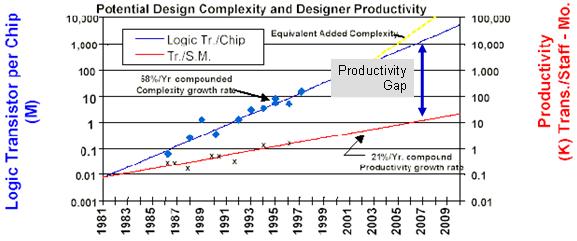
The reason for increasing design complexity is multifold – decreasing geometries allow designers to add more and more elements to the chip, making the entire process challenging. Number of IP cores per chip has grown from ~30 in 2003 to over 250 in 2006 and possibly much more today (source: EETimes). In addition, a big bull’s eye has been painted on power consumption numbers and most chips now must be designed using low power techniques. Plus, increasing complexity means that chip verification becomes more complex; 50% of all ASIC designs today require respins due to functional/logic errors (Source: Colette International Research).

Rather than a single solution, it is very likely that a multitude of innovative solutions that address individual problems will emerge. For example, better modeling techniques that can give a very accurate QoR estimate at the architecture stage itself can reduce the design complexity downstream. Languages such as SystemVerilog literally reduce the lines of code that a designer or verification engineer must write, thus boosting productivity. Time also may be right for ESL design, which has been around for a while, as conventional techniques fail to keep up.

All in all, we live in very interesting times. Faster and smaller is not always for the better. The industry must innovate and rise up to the economic and design challenges if it is to survive and prosper.

Reblog this post [with Zemanta]

Too Soon to call for a Semiconductor Recovery?

(This post by Abhijit Athavale, the driving force behind PuneTech’s PuneChips forum, is cross-posted from his blog.)

Are we really out of the most dreaded recession after the great depression and on our path to recovery? The answer might be a resounding yes if we look at the recent crop of earnings reports from technology companies, and other data emerging from market analysis firms. In fact, the NASDAQ composite is already into deeply positive territory on the expectations of an imminent recovery.

Revenue and Inventory Declines from 2008 to 2009

However, a quick dissection of recent earnings announcements from a few prominent semiconductor companies shows that we are not out of the woods yet. The chart above shows that sales numbers are still horribly bad compared to last year, and inventories have declined sharply as well. This means that companies have managed to satisfy the underlying demand by using up their inventories, and will or already have started ordering replacement units from fabs. This explains why the fabs have reported better numbers than the IC vendors. In a normal growth phase, every company wants to keep its channel well stocked to feed demand. This is not the case now as companies are drawing down on finished stock to reduce costs and improve margins. So much for the expected recovery in demand …

Where does this demand come from ultimately? The consumer, of course. The US, Europe (as a whole) and Japan are the three largest economies in the world.

People living in these countries constantly keep (or, at least used to) buying new things such as laptops and PCs, cell phones, gaming consoles, automobiles, audio and video equipment, personal media players, TVs, toys, and other gadgets. Companies that manufacture consumer electronics ICs directly feed this demand. Consumers also buy services such as wireless and wireline voice and data, broadband, cable and satellite TV feeds. This in turn generates demand for the entire telecom, datacom and wireless infrastucture and service providers. Infrastructure IC manufacturers are responsible for suppplying this demand. In the US alone, the consumer is 70% of the entire economy. The consumer is also a major portion of the EU and Japanese economies. The consumption in all three major economies in the world has cratered, as evidenced by the continuous 6 to 9 month declines in the exports from China, Taiwan and Japan, major export reliant countries.

The real demand will not be back till the consumer starts spending again. And, that is almost impossible in this economy. Take the US for example – official unemployment is at ~11% (some say, it is near 16% unofficially), one in ten homeowners is underwater, and credit lines have been severely downgraded by banks. Three major sources of funds used by consumers have been seriously compromised. To use a banking term, the consumer is now de-leveraging and getting his house in order. There will be no more spending sprees till the US savings rates are back to historical levels. The EU and Japan are in even worse situations as their banks are still over leveraged and that still needs to be played out a la Bear Sterns and Lehman Brothers.

My belief is that the semiconductor industry and the companies that serve the semiconductor industry are not coming back till personal finances get better. That is not likely to happen for a while. Some analysts are calling Q2, 2009 as the bottom, which very well may be so, but I don’t expect to see a quick recovery from this point on. In fact, the worsening unemployment and foreclosure numbers may push us back into a double dip recession. If not, the recovery will be tepid and totally unspectacular.

Reblog this post [with Zemanta]

PuneChips Editor’s Blog – Second Edition

First, an update on PuneChips – we now have 5465 members in the Linked In group and over 40 in the Google Groups mailing list. Some folks doing applications work have also joined us. Given that there are 300 or so semiconductor designers in the Pune area, and hundreds more developing applications, we have ways to go.

On Monday, June 29th, we had our second event; a speech by Shrinath Keskar, former M.D. of Ikanos Communications in India. A good cross section of people attended the event and the discussion was quite lively. We had several new faces in the room, a definitive indicator of progress.

We also have our first guest blog written by Chaitanya Rajguru of KPIT Cummins Infosystems, and this is really what we are looking for. I want more people to participate in group discussions and idea generation. Rather than having only just a handful of people writing content, involvement from all is needed if we want to keep growing and have a voice in the development of Pune as a Chip/Embedded design hub.

Shrinath spoke about the challenges of designing chips for the telecom sector. The topic was quite relevant since we have several companies in the area that service Telecom applications. Shrinath not only focused on design challenges which generally revolve around the cost/power/features triangle, but also on challenges offered by the market; telecom standards, time to market and deployment. This was good information for engineers as it explained the logic behind many management decisions.

Telecom standards, both wireline and wireless, drive how telecom companies go about their business. Standards not only have technical, but regulatory challenges associated with them. In addition, there are competing standards that try to solve the same problem (Fig 1) and technical slugfests go on for many years before a winner emerges.

Figure 1: Plethora of Wireless Standards, Source: Nokia

Many a times, the winning standard has such a short window of opportunity that it may be pointless to keep designing to it. Sometimes, governments propose standards in order to get access to advanced technology; China proposed WAPI a few years ago for wireless security. The catch was that anyone trying to sell Telecom equipment in China would have to disclose their technology to a Chinese partner if (emphasis is mine) WAPI had been adopted.

In order to support current and possibly future standards, chips have to be intelligently designed with possibly some redundant I/O, memory and cells which can be used to fix design faults or adapt to changing standards. Figure 2 below shows what a chip designer spends doing day in and out and to Shrinath’s point, there are lots of opportunities available for innovators to improve the design process – innovation does not need to end at the transistor level.

Figure 2: Where a Designer Spends All His Time, Source: Xilinx, 2004

Telecom equipment typically stays in the market for years as telecom standards take a while to roll out due to regulatory or geographical hurdles. However, a chip vendor hardly ever has that kind of time to supply the product. A telecom line card will be generally designed in 9-12 months and the chip must be designed, tested and deployed in the production line card within that timeframe. Time to Market is very important for Telecom OEMs; hence chip vendors must be able to convert design wins into production chips that work.

Deployment is a very important phase in the life of a telecom chip. You can test the product in labs that mimic customer test environments, but you can never test for real situations such as interference from out of spec frequency bands. It is very important to have good support staff on hand to fight these battles alongside customers. Your chip must work in each and every deployment; even a 90% success rate will not cut it.

As Moore’s law comes to the end of life, there is a lot of discussion happening around a new sustainable model for chip startups. The current model, which requires upwards of $50M in VC money to be profitable, cannot live for long. Very likely, the next invention in the semi/EDA market is going to be economic, something that allows new companies to form and prosper.

Abhijit Athavale
PuneChips Editor

Reblog this post [with Zemanta]

Event: IC Design Challenges in the Telecom sector – Shrinath Keskar, ex-MD Ikanos, India – 29th June

The integrated circuit from an Intel 8742, a 8...
Image via Wikipedia

What: Talk by Shrinath Keskar, fomer MD Ikanos Communications India, on IC Design Challenges in the Telecom Sector.
When: Monday, 29th June, 6:30pm to 8:00pm
Where: Venture Center, NCL Innovation Park, Pashan Road. To reach Venture Center, go past NCL towards Pashan, pass the cricket ground adjacent to NCL and then you’ll find NCL Innovation Park / Venture Center on the right hand side. Map
Registration and fees: This event is free for all to attend. No registration required.

About the speaker – Shrinath Keskar

Shrinath Keskar, former M.D. of Ikanos Communications of India has over 17 years of experience in the field of Semiconductors. He joined Ikanos in the year 2000 and has been with the company since then. Shrinath also worked with Fortune 500 hindered companies such as Motorola and Sun Microsystems before joining Ikanos. He has a Master’s degree in Computer Engineering from Texas A &M and B.E. from College of Engineering, Pune.

About PuneChips

PuneChips is a special interest group on semiconductor design and applications. This event is the inaugural event for PuneChips. PuneChips was formed to foster an environment for growth of companies in the semiconductor design and applications segment in the Pune area. Our goal is to build an ecosystem similar to PuneTech for companies in this field, where they can exchange information, consult with experts, and start and grow their businesses.

For more information, see the PuneTech wiki profile of PuneChips, and/or join the PuneChips mailing list.

Please forward this mail to anybody in Pune who is interested in semiconductors, chip design, VLSI design, chip testing, and embedded applications.

Reblog this post [with Zemanta]

PuneChips Weekly Roundup: Nortel, Moore’s Law, Graphene, 3G and more

(This is a roundup of last week’s semiconductor/EDA industry news by Abhijit Athavale founder/editor of PuneChips – Pune’s forum for the semiconductor industry. For more information about PuneChips see the PuneTech wiki profile of PuneChips)

The integrated circuit from an Intel 8742, a 8...
Image via Wikipedia

Please keep the responses coming. It is encouraging to see that as a writer. Last week’s mention goes to Sagar Khedkar, who picked out Iranian Politics 101 as the OT item. Congratulations!

Last week was pretty packed from a news standpoint so the newsletter is a little long as well.

Markets

  • Nortel done for good: Nortel has sold off whatever was remaining to Nokia Siemens Networks. I remember the days when Nortel was one of biggest OEM customer for a majority of semiconductor companies. No more, RIP!
  • More on Moore!

    While the demise of Moore’s law has been predicted many times, will this prediction be true? Could be, if you are thinking that the cost per transistor will decline due to process geometries. However, there may be other methods of reducing the cost other than using a smaller process node. Some out of the box or lateral thinking may be needed to keep Moore’s law alive.

    BTW, a little birdie told me that 2014 will unleash a new economic up-wave much like 1999. I wonder if that will again be based on advances in the semiconductor/nano-tech fields.

  • KPMG to pay Vitesse $22.5M in settlement: This has to be the first of its kind. Collusion with the management to doctor financial statements doesn’t pay anymore
  • Semiconductor Market updates: There are just too many of those every week so rather than adding links, I will just summarize. The curious readers can go find the articles themselves
    • Gartner is claiming that the semi market has hit the bottom and is increasing capex outlook. I wonder if they will have to eat their words. Gartner is also saying that IT spending will fall 3.8% this year, but grow by 2.4% next year – I just don’t understand how this works; if the biggest downturn after the great depression can cause a decline of 3.8%, a bounceback of 2.4% next year would absolutely have to be backed up by heady growth, which does not seem likely.
    • iSuppli says that semi sales were pretty bad last quarter, but like Gartner is calling Q1, 2009 as the bottom and saying that Q4, 2009 will be better than Q4, 2008. We shall see ….
    • Japan fab tool book to bill has climbed from 0.65 in April to 0.74 in May. Again the claim is that we have reached the bottom. How do we get this number? The three month average for worldwide billing was $391.1M in May while it was $385.7M in April. This does not really seem to be a quantitative improvement and to call a bottom based on this certainly does seem to be a leap of faith.

    In general, people are trying to be optimistic. However, I am not sure that we are going to see any quantitative improvement even if we are at a bottom. We could be at the bottom for a long time. Forget these numbers and just look at Chinese and Japanese exports for the past few months – they have fallen in May as well. That tells me that there is no one buying those chips that people are making!

  • Analog Devices launches a new website: This is a prime example of marketing people creating news of out nothing and the press covering it. I wonder if ADI also held press briefings to herald the advent of a new website to the editors.
  • India’s Solar plans: Going by the past record in power generation, I will be happy even if we see 1% of the 1GW power generation target
  • New Energy guidelines for the US and the EU: Now this is something I wholeheartedly support. Government regulation in this case will spur innovation and reduce power consumption, possibly giving better returns to the companies. According to the news item, energy start rated appliances saved ~$19b from the US energy expenditure costs.

PC/Processor

  • Sun may cancel Rock, a high-end Server CPU: The Rock may turn into a Brick as Sun failed to submit a paper at the HotChips conference. They should really give up the pretense. They have lost the battle and the war and need to focus on something that they do really well.
  • EU warns Microsoft against not including the browser in Windows 7: Microsoft seems to be caught between a rock (pun not intended) and a hard place. After punishing them for including IE with WIndows, now the EU is telling them not including the browser will be a problem as well. Instead, they should include a choice of browsers with the OS, albeit tested, so the lazy bums on the EU competition commission don’t have to download and install.

Mobile

  • India sets 3G base fee at $835M: Get on with this already. We are tired and waiting to get 3G. While I am not sure, this may be the first instance where mobile companies have the 3G networks ready, but the spectrum is not. No wonder the Indian Bureacrats were ranked way at the bottom.
  • First look at iPhone 3GS: Looking at the Broadcom and Toshiba chips inside, people are saying that the “S” stands for Savings …

Storage

Technology

That’s all for this week …

Reblog this post [with Zemanta]

PuneChips weekly roundup: Marketing ‘green’, Power over Ethernet and more

(This is a roundup of last week’s semiconductor/EDA industry news by Abhijit Athavale founder/editor of PuneChips – Pune’s forum for the semiconductor industry. For more information about PuneChips see the PuneTech wiki profile of PuneChips)

The integrated circuit from an Intel 8742, a 8...
Image via Wikipedia

Thank you for the great response to last week’s e-mail. Please continue with your responses and I will keep on sending this out every week.

Arati Halbe gets the mention for being the first one to pick on the OT news from last week. A few other people did point it out as well, but she was the first. Another reader thought that the Semi industry in Pune is like the Mayan Civilization as it keeps on depleting local resources, and hence the topic was really on the money 🙂 This newsletter also contains an OT item, but is more entertaining.

Markets

  • Google and the Internet caused economic crisis: This brilliant conclusion drawn by Peter Clarke of EE Times. While it is true that globalization and improved communication technologies have disrupted traditional economies, by the same token the Industrial revolution disrupted existing agrarian economies and can be blamed for the great depression. So, while the headline is catchy, the conclusion is just plain wrong …
  • Are we in denial about the crappy semiconductor market: iSuppli says that foundry market will see strong growth in Q2 after three straight quarters of contraction, but FBR said that the market will cool off in Q3. Why the bullish tone? Does it really matter that the IC market declined by 22% against 24%? It still is terrible and unless and until the cost structures created to support higher sales numbers are dismantled, we will not see 1990’s type growth. Short term thinking to please the wall street is the real culprit here. There are innumerable news items last week that herald a recovery, but is it real? I have nothing against a recovery, but I just don’t get how people will start buying more chips when they are just not buying anything at all? Gartner clearly says that the demand has not returned to the market and increased sales for some companies are due to inventory restocking – this is also known as stuffing the channel. (link)

PC/Processor

Mobile

Storage

  • Broadcom wants confidential information from Emulex: Does this not sound a little odd? Why would anyone give up their confidential information to a hostile buyer? Broadcom seems to have painted itself in a corner with no way of getting out. The market is also pricing Emulex above the Broadcom offer.

Technology

  • Power over Ethernet market sees growth: Now what would be interesting is to see if someone could send power packets over wireless Ethernet. That will instantly get rid of all the clutter we have around our PCs. Let’s see if that can be done without frying anything that gets in the way!
  • Nokia demonstrates energy harvesting handset: Hey, I was not that far off. Hopefully, laptops can also be charged in the same way not too far in the future.
  • ZigBee & low power Bluetooth tapped as the next generation health device standard: This is really important as networked health devices are going to be a huge market. Imagine a blood pressure monitor sending a message to your doctor when irregularities are seen. I think this is a fabulous opportunity for Indian companies to be developing health devices. However, Bluetooth is far from reliable and has too many connectivity issues so they will hopefully have been fixed.
  • Thin Film Batteries are here: This could be a solid advance in reducing device sizes even further.

That’s all for this week …

Reblog this post [with Zemanta]

PuneChips: Weekly round-up of Semiconductor/EDA News

(This is a roundup of last week’s semiconductor/EDA industry news by Abhijit Athavale founder/editor of PuneChips – Pune’s forum for the semiconductor industry. For more information about PuneChips see the PuneTech wiki profile of PuneChips)

The integrated circuit from an Intel 8742, a 8...
Image via Wikipedia

This is my first attempt at sending out a digest of Semi/EDA news from last week. I am also peppering it with my own, slightly irreverent comments, so feedback from you is greatly appreciated. I will also try to put in at least one off topic item somewhere just to see if you are reading this! Whoever points out the OT item, will get a reward – your name will get a mention in next week’s news.

Markets

PC/Processor

  • Intel buys Windriver for $884 million: Possible that Intel is now targeting embedded apps. I wonder if they will launch another crush operation against Motorola (Freescale now). This on the heels of the rumor that Nvidia is thinking about a new x86 based processor.
  • Microsoft to exclude ARM based netbooks from Windows 7: Is that a surefire way of making sure that ARM based netbooks don’t get popular with the non-geeky crowd?
  • Larry Ellison wants more Java on Netbooks and Phones: Here goes Larry again. Anyone remember his attempt at pushing a network PC a few years ago? A PC or a phone either has Java or not – how do you get more or less Java? And, I don’t think he intends to spill Coffee on the machines 🙂
  • Intel launches the CULV Processor: What is a CULV – this is just as bad as BING. Wonder if Intel and MSFT used the same agency to come up with the respective names. China may be the main market for this, so they are probably betting on getting this pronounced as CURVE anyway.

Mobile

Storage

Technology

  • Flexible Memory: The researchers at National Institute of Standards and Technology in the US claim that this technology can be used to print memory as easily as printing a slide. I can’t wait for the day when I add more memory to my machine by photocopying it at the neighborhood store …
Reblog this post [with Zemanta]

PuneChips Editor’s Blog: PuneChips Inaugural Event

Well, I am quite excited to get the PuneChips forum up and running. While we would have liked to see more people attend, we had a good start. We invited most of the Semi/EDA folks in and around Pune and did get a very favorable response. Pending work and travel schedules are probably the culprits for a lower attendance, and I certainly hope that we will get more and more people to attend future events.

Ultimately, this forum is for the Semiconductor/EDA and Applications companies in and around Pune and we want to make sure that all future events/programs are catered to these companies needs. Again suggestions are most welcome and we are most certainly looking for individuals and companies to take on other responsibilities. We already have a taker for writing a guest blog so that is an encouraging sign.

That said I want to thank Abhijit Abhyankar from Rambus for taking time out of his busy schedule to present to us. The presentation was packed with lots of information generated a healthy amount of discussion during and after. Abhijit mentioned falling productivity and increasing power consumption as the two most important industry challenges, and therein lie the opportunities. Due to progressively declining geometries, number of transistors per chip has exploded, creating all sorts of new challenges. Conventional problem solving approaches are not working and radically different methodologies are required.

Chart of Sematech Potential Design Complexity and Designer Productivity in Semiconductors

Ever since Gordon Moore made his empirical observation that transistor densities will double every two years, the industry has been making concerted efforts to ensure that Moore’s law remains valid despite all predictions otherwise. Physical limits do certainly pose a challenge to increasing the transistor densities in two dimensions, but scientists are working on 3D placement of transistors, where transistors are either placed vertically, or on top of each other. Another approach to increase densities is to skip the third dimension altogether and go directly to the fourth, i.e. Time. Some programmable device makers think that you can make a cell or logic block on the chip perform different functions during a clock cycle resulting in extremely dense chips without pushing physical limits. If these efforts are successful, Moore’s law will continue to live for a long time.

Interestingly, Google’s founder Sergey Brin came up with a new term coined “Page’s Law” (watch this clip) named after his co-founder just last month. It states that software gets twice as slow every 18 months, explaining why your cell phones and PCs seem slower even as the HW inside remains unchanged. This new law seems to be destined as a sidekick of Moore’s law and may provide a reason for people to go buy new hardware every 18 months! Maybe, this is what they call a virtuous cycle …

Jokes aside, productivity and power are certainly a couple of areas that need solving in the near term. SEMATECH or Semiconductor Manufacturing Technology Association has circulated this interesting chart which compares design complexities to designer productivity. This problem can certainly be solved by creating new tools that let the designer work from a much higher level than delving deep within the IC.

Additionally, today’s chips consume too much power. Power analysis has become a huge time sink during chip design due to very high densities. It may not be an overestimation to claim that power related issues are a major cause of productivity losses during chip design. Newer techniques that allow designers to work on reducing power from the early design stages are required, in addition to new architectures that inherently consume less power.

I personally feel that Indian companies should rise up to solve this challenge. While we are not well set as far as semiconductor manufacturing goes, we are certainly on the ball with respect to VLSI design, verification, simulation, etc. We have the talent, the training and now, even the experience to tackle these challenges. To all the young entrepreneurs out there, look at the evolving opportunities in this sector; there certainly is a world beyond web 2.0.

Finally big thanks to Kaushik Gala and the NCL Venture Center for opening up their facilities to this group. Rarely do we see such well equipped meeting rooms and fabulous campuses. I also want to thank everyone who attended the inaugural event. We had some very senior people attend from QLogic, LSI, and KPIT Cummins. There are 12-13 more companies in the area and I would really like to encourage engineers working there to attend. There will be lots of opportunities to learn from industry experts, network and formulate your ideas. Keep in mind that we will not be able to distribute yesterday’s presentation to a wider audience so those that did not attend truly missed out. I expect this will happen in the future due to corporate guidelines, so it is important that people show up for the event.

Once again, thanks to everyone who helped get PuneChips off the Ground.

If you’re a technology professional interested in the semiconductor/EDA area in Pune, please join the PuneChips mailing list and linked-in group.

About the Author – Abhijit Athavale

Abhijit Athavale is the President and CEO of Markonix, and a high-tech marketing consultant. He has 16+ years of high-technology industry experience. Prior to Markonix, Abhijit spent over 11 years at Xilinx, Inc. in various engineering, applications and marketing roles. In his role as a marketing consultant, he has held executive management positions at Taray, Inc and Sanved DA. He has a masters degree in electrical engineering from Texas A&M University and a bachelors degree in electrical engineering from University of Pune. He is an accomplished speaker and author of several publications including a book.

Reblog this post [with Zemanta]