First, an update on PuneChips – we now have 5465 members in the Linked In group and over 40 in the Google Groups mailing list. Some folks doing applications work have also joined us. Given that there are 300 or so semiconductor designers in the Pune area, and hundreds more developing applications, we have ways to go.
On Monday, June 29th, we had our second event; a speech by Shrinath Keskar, former M.D. of Ikanos Communications in India. A good cross section of people attended the event and the discussion was quite lively. We had several new faces in the room, a definitive indicator of progress.
We also have our first guest blog written by Chaitanya Rajguru of KPIT Cummins Infosystems, and this is really what we are looking for. I want more people to participate in group discussions and idea generation. Rather than having only just a handful of people writing content, involvement from all is needed if we want to keep growing and have a voice in the development of Pune as a Chip/Embedded design hub.
Shrinath spoke about the challenges of designing chips for the telecom sector. The topic was quite relevant since we have several companies in the area that service Telecom applications. Shrinath not only focused on design challenges which generally revolve around the cost/power/features triangle, but also on challenges offered by the market; telecom standards, time to market and deployment. This was good information for engineers as it explained the logic behind many management decisions.
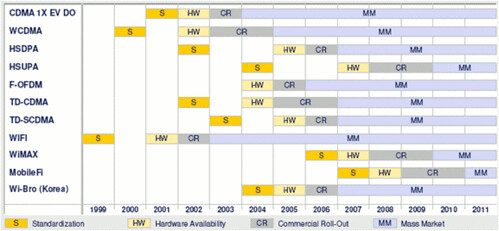
Telecom standards, both wireline and wireless, drive how telecom companies go about their business. Standards not only have technical, but regulatory challenges associated with them. In addition, there are competing standards that try to solve the same problem (Fig 1) and technical slugfests go on for many years before a winner emerges.

Many a times, the winning standard has such a short window of opportunity that it may be pointless to keep designing to it. Sometimes, governments propose standards in order to get access to advanced technology; China proposed WAPI a few years ago for wireless security. The catch was that anyone trying to sell Telecom equipment in China would have to disclose their technology to a Chinese partner if (emphasis is mine) WAPI had been adopted.
In order to support current and possibly future standards, chips have to be intelligently designed with possibly some redundant I/O, memory and cells which can be used to fix design faults or adapt to changing standards. Figure 2 below shows what a chip designer spends doing day in and out and to Shrinath’s point, there are lots of opportunities available for innovators to improve the design process – innovation does not need to end at the transistor level.

Telecom equipment typically stays in the market for years as telecom standards take a while to roll out due to regulatory or geographical hurdles. However, a chip vendor hardly ever has that kind of time to supply the product. A telecom line card will be generally designed in 9-12 months and the chip must be designed, tested and deployed in the production line card within that timeframe. Time to Market is very important for Telecom OEMs; hence chip vendors must be able to convert design wins into production chips that work.
Deployment is a very important phase in the life of a telecom chip. You can test the product in labs that mimic customer test environments, but you can never test for real situations such as interference from out of spec frequency bands. It is very important to have good support staff on hand to fight these battles alongside customers. Your chip must work in each and every deployment; even a 90% success rate will not cut it.
As Moore’s law comes to the end of life, there is a lot of discussion happening around a new sustainable model for chip startups. The current model, which requires upwards of $50M in VC money to be profitable, cannot live for long. Very likely, the next invention in the semi/EDA market is going to be economic, something that allows new companies to form and prosper.
Abhijit Athavale
PuneChips Editor
![Reblog this post [with Zemanta]](http://img.zemanta.com/reblog_b.png?x-id=f578279b-a1c0-4bec-8cd2-6229d5905f16)