Tag Archives: semiconductors

PuneChips event: Wavelet Transform & its Applications in Image Processing – 6th March

(This article about a PuneChips event is reproduced with permission from the PuneChips website)

What: Talk by Ganesh Bhokare on Wavelet Transform & its Applications in Image Processing
When
: Saturday, 6th March 2010, 10:00 am to 12:00 noon.
Where: Venture Center, NCL Innovation Park, Pashan Road
Registration and fees: This event is *FREE* for all to attend. No registration required.

PuneChips is a PuneTech special interest group on semiconductors, VLSI, embedded, and EDA. Click on the image to see all PuneTech articles about PuneChips
An image of a two level wavelet transform. A PuneChips event, on the Wavelet Transform and its applications in Image Processing will be held in Venture Center on 6th March. PuneChips is a PuneTech special interest group on semiconductors, VLSI, embedded, and EDA. Click on the Logo to see all PuneTech articles about PuneChips. Image by Alessio Damato via Wikipedia.

Wavelet Transform & its Applications in Image Processing

In today’s multimedia wireless communication , major issue is bandwidth needed to satisfy real time transmission of audio and video data. The solution to this problem is to efficiently compress audio and video data for a given SNR. Wavelet transform is an evolving technology which offers far higher degrees of data compression compared to standard transforms such as DCT etc. In this talk we will be discussing concepts of wavelet transform and its applications to image compression and processing. The same can be extended to video processing.

About the speaker – Ganesh Bhokare

Ganesh Bhokare has over 15 years experience in using DSP audio, video and Embedded systems for Digital Media Processing. He is a PhD candidate at IIT Mumbai and currently in the process of defending his thesis. He has professional experience with  NXP, Conexant, TI and Cirrus Logic.

About Venture Center

Entrepreneurship Development Center (Venture Center) – a CSIR initiative – is a not-for-profit company hosted by the National Chemical Laboratory, Pune. Venture Center strives to nucleate and nurture technology and knowledge-based enterprises by leveraging the scientific and engineering competencies of the institutions in the Pune region in India. The Venture Center is a technology business incubator specializing in technology enterprises offering products and services exploiting scientific expertise in the areas of materials, chemicals and biological sciences & engineering.

About PuneChips

PuneChips is a special interest group on semiconductor design and applications. PuneChips was formed to foster an environment for growth of companies in the semiconductor design and applications segment in the Pune area. Our goal is to build an ecosystem similar to PuneTech for companies in this field, where they can exchange information, consult with experts, and start and grow their businesses.

For more information, see the PuneChips website at http://punechips.com, and/or join the PuneChips mailing list: http://groups.google.com/group/punechips.  Please forward this mail to anybody in Pune who is interested in renewable energy, solar technologies, semiconductors, chip design, VLSI design, chip testing, and embedded applications.

Reblog this post [with Zemanta]

Comments are closed on this article. Please comment at the original article

PuneChips Editor’s Blog: PuneChips Inaugural Event

Well, I am quite excited to get the PuneChips forum up and running. While we would have liked to see more people attend, we had a good start. We invited most of the Semi/EDA folks in and around Pune and did get a very favorable response. Pending work and travel schedules are probably the culprits for a lower attendance, and I certainly hope that we will get more and more people to attend future events.

Ultimately, this forum is for the Semiconductor/EDA and Applications companies in and around Pune and we want to make sure that all future events/programs are catered to these companies needs. Again suggestions are most welcome and we are most certainly looking for individuals and companies to take on other responsibilities. We already have a taker for writing a guest blog so that is an encouraging sign.

That said I want to thank Abhijit Abhyankar from Rambus for taking time out of his busy schedule to present to us. The presentation was packed with lots of information generated a healthy amount of discussion during and after. Abhijit mentioned falling productivity and increasing power consumption as the two most important industry challenges, and therein lie the opportunities. Due to progressively declining geometries, number of transistors per chip has exploded, creating all sorts of new challenges. Conventional problem solving approaches are not working and radically different methodologies are required.

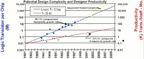
Chart of Sematech Potential Design Complexity and Designer Productivity in Semiconductors

Ever since Gordon Moore made his empirical observation that transistor densities will double every two years, the industry has been making concerted efforts to ensure that Moore’s law remains valid despite all predictions otherwise. Physical limits do certainly pose a challenge to increasing the transistor densities in two dimensions, but scientists are working on 3D placement of transistors, where transistors are either placed vertically, or on top of each other. Another approach to increase densities is to skip the third dimension altogether and go directly to the fourth, i.e. Time. Some programmable device makers think that you can make a cell or logic block on the chip perform different functions during a clock cycle resulting in extremely dense chips without pushing physical limits. If these efforts are successful, Moore’s law will continue to live for a long time.

Interestingly, Google’s founder Sergey Brin came up with a new term coined “Page’s Law” (watch this clip) named after his co-founder just last month. It states that software gets twice as slow every 18 months, explaining why your cell phones and PCs seem slower even as the HW inside remains unchanged. This new law seems to be destined as a sidekick of Moore’s law and may provide a reason for people to go buy new hardware every 18 months! Maybe, this is what they call a virtuous cycle …

Jokes aside, productivity and power are certainly a couple of areas that need solving in the near term. SEMATECH or Semiconductor Manufacturing Technology Association has circulated this interesting chart which compares design complexities to designer productivity. This problem can certainly be solved by creating new tools that let the designer work from a much higher level than delving deep within the IC.

Additionally, today’s chips consume too much power. Power analysis has become a huge time sink during chip design due to very high densities. It may not be an overestimation to claim that power related issues are a major cause of productivity losses during chip design. Newer techniques that allow designers to work on reducing power from the early design stages are required, in addition to new architectures that inherently consume less power.

I personally feel that Indian companies should rise up to solve this challenge. While we are not well set as far as semiconductor manufacturing goes, we are certainly on the ball with respect to VLSI design, verification, simulation, etc. We have the talent, the training and now, even the experience to tackle these challenges. To all the young entrepreneurs out there, look at the evolving opportunities in this sector; there certainly is a world beyond web 2.0.

Finally big thanks to Kaushik Gala and the NCL Venture Center for opening up their facilities to this group. Rarely do we see such well equipped meeting rooms and fabulous campuses. I also want to thank everyone who attended the inaugural event. We had some very senior people attend from QLogic, LSI, and KPIT Cummins. There are 12-13 more companies in the area and I would really like to encourage engineers working there to attend. There will be lots of opportunities to learn from industry experts, network and formulate your ideas. Keep in mind that we will not be able to distribute yesterday’s presentation to a wider audience so those that did not attend truly missed out. I expect this will happen in the future due to corporate guidelines, so it is important that people show up for the event.

Once again, thanks to everyone who helped get PuneChips off the Ground.

If you’re a technology professional interested in the semiconductor/EDA area in Pune, please join the PuneChips mailing list and linked-in group.

About the Author – Abhijit Athavale

Abhijit Athavale is the President and CEO of Markonix, and a high-tech marketing consultant. He has 16+ years of high-technology industry experience. Prior to Markonix, Abhijit spent over 11 years at Xilinx, Inc. in various engineering, applications and marketing roles. In his role as a marketing consultant, he has held executive management positions at Taray, Inc and Sanved DA. He has a masters degree in electrical engineering from Texas A&M University and a bachelors degree in electrical engineering from University of Pune. He is an accomplished speaker and author of several publications including a book.

Reblog this post [with Zemanta]

Emerging opportunities in the semiconductor industry – with Abhijit Abhyankar, country head Rambus India – 4th June

PuneTech logoWhat: Talk by Abhijit Abhyankar, country head of Rambus India, on the current trends in the semiconductor industry and emerging opportunities in the areas of IC design, EDA tools and applications.
When: Thursday, 4th June, 6:30pm to 8:00pm
Where: Venture Center, NCL Innovation Park, Pashan Road. To reach Venture Center, go past NCL towards Pashan, pass the cricket ground adjacent to NCL and then you’ll find NCL Innovation Park / Venture Center on the right hand side. Map
Registration and fees: This event is free for all to attend. No registration required.

About the speaker – Abhijit Abhyankar

Abhijit Abhyankar is a Sr. Engineering Director, and the country head for Rambus Chip Technologies, India. Abhijit has over 17 years of industry experience and was directly involved in the design of groundbreaking Rambus memory technology. He has held various engineering, management and executive positions at Rambus. He has authored several publications and is the inventor of multiple patented technologies at Rambus. Abhijit has an MBA degree from San Jose University, an MSEE from Stanford University and a BSEE from University of Utah.

About PuneChips

PuneChips is a special interest group on semiconductor design and applications. This event is the inaugural event for PuneChips. PuneChips was formed to foster an environment for growth of companies in the semiconductor design and applications segment in the Pune area. Our goal is to build an ecosystem similar to PuneTech for companies in this field, where they can exchange information, consult with experts, and start and grow their businesses.

PuneChips has been started by Abhijit Athavale, president and CEO of Markonix, and a high-tech marketing consultant. He has 16+ years of high-technology industry experience. Prior to Markonix, Abhijit spent over 11 years at Xilinx, Inc. in various engineering, applications and marketing roles. In his role as a marketing consultant, he has held executive management positions at Taray, Inc and Sanved DA. He has a masters degree in electrical engineering from Texas A&M University and a bachelors degree in electrical engineering from University of Pune. He is an accomplished speaker and author of several publications including a book.

For more information, see the PuneTech wiki profile of PuneChips, and/or join the PuneChips mailing list.

Please forward this mail to anybody in Pune who is interested in semiconductors, chip design, VLSI design, chip testing, and embedded applications.

Reblog this post [with Zemanta]

India/China better markets today for tech startups – Ajit Shelat, SVP, Nevis Networks

Ajit Shelat Nevis Networks
Ajit Shelat, Senior Vice President of Engineering, Nevis Networks

Nevis Networks, a mostly-Pune-based-company (with “official” headquarters in the US, and an additional center in China), builds network switches and other network hardware that allows a company to secure it’s internal network from attacks and to enforce identity-based security policies. The company’s LANenforcer product family transparently protects the network from external malicious attacks, and also allows restricting access to different network resources based on users’ identities according to policies set by the system administrators. This can be customized to ensure different levels of access to different classes of users, employees, contractors, guests and other third parties. In addition, the product allows detailed reporting, auditing, employee activity reports that make it possible to analyze security breaches in very granular detail. And because it is hardware based, all of this is delivered in realtime with very low latency.

Nevis Networks’ customers range from financial services, healthcare, education and defense contractors and they deploy Nevis LANenforcers to protect sensitive network resources and assets, with an intention of reducing the overall costs and time to resolve security breaches and conduct network audits. The company is headquartered in Mountain View, CA, with additional R&D centers in Pune, India and Beijing, China.

The ongoing recession has hit Nevis Networks hard, and it downsized a very large fraction of its workforce late last year. On top of that, on Monday, in a report title “LSI Acquires Manpower Team of Navis Networking”, CXOToday implied that the company (which they alternately identified as Navis Networks or Nevis Networks in the article) had shutdown and the team taken over by LSI. Specifically, this is what CXOToday said:

With recession being an opportunity to invest for big MNCs, LSI Technologies, a provider of innovative silicon, systems and software technologies has acquired the team of Navis Networking based at Pune. With the R&D unit based out of Mountain View, California shutting down, LSI has acquired the manpower of the captive R&D centre in India.

After hearing from PuneTech readers that this report is misleading, we caught up with Ajit Shelat, Senior Vice President of Engineering for Nevis Networks, to learn that the reports of Nevis’ demise have been greatly exaggerated. Here is a quick report of the conversation we had with Ajit:

On the news that LSI has “acquired” the “manpower” of Nevis but not the company.

The report by CXOToday is misleading. What actually happened is much simpler. Due to the economic downturn last year, Nevis Networks was looking to downsize some of its workforce. A friendly interaction between the respective managements of Nevis and LSI led to movement of some of Nevis manpower to LSI. This was a simple case of Nevis ex-employees being hired by LSI en masse. It does not represent any sort of acquisition or even agreement between Nevis and LSI. And these are certainly not the entire team of Nevis Networks India, as implied by the CXOToday article.

In any case, Nevis networks is not shutting down. It continues to execute on a with strategy and focus.

On the current status of Nevis Networks

Nevis networks core team is still there and it is going strong. In fact, the last quarter was quite good and has been the best quarter for Nevis since the inception of the company.

What has happened is that due to the downturn, Nevis shifted its focus away from the US market to the India and China markets, reduced its workforce in the US and in India, and this new strategy appears to be working for them.

On the surprising fact that India/China are better markets than the US market

Since Nevis Networks is selling cutting edge technology, one would have expected US to be the logical market for these products. However, people really underestimate the extent of the effect the economic recession is having on the market there. While the markets really melted around September 2008, the signs have been obvious for at least an year before that, and starting Nov/Dec 2007, Nevis had started planning its strategy of shifting focus away from the US market to the India/China markets.

In tune with their new strategy, Nevis substantially reduced its India workforce. They continue to support existing customers in the US, but new customers are coming mainly from India – which is apparently not affected by the recession as much. In general, it is easier for a company with mainly Indian promoters to sell in India than in other countries.

China is another country where sales are expected to grow – Nevis is in the process of stengthening its sales presence in China. The Chinese market, having a significantly different character, takes a longer ramp up time to achieve its full potential – though a very good start has been made in terms of immediate sales. Like other markets, achieving full potential is really a function of getting the right people on the ground, and building the right relationships and customer confidence. All this effort is justified by the fact that the Chinese market has the potential to scale up dramatically.

More about Nevis Networks

Nevis Networks was founded in 2002 with the intention of building a network security solution with high speed and low latency, using its proprietary ASIC-based technology. As of last year, Nevis had raised a total of US$40 million in three rounds of funding from premier venture capital firms New Enterprise Associates, BlueRun Ventures (formerly Nokia Venture Partners) and New Path Ventures LLC. We are told that their funding situation has recently changed and an announcement to this effect is expected in the next couple of weeks.

Reblog this post [with Zemanta]

Narendra Karmarkar’s recent research

After working on the Interior Point Method, Karmarkar worked on a new architecture for supercomputing, based on concepts from projective geometry. Currently, he is synthesizing these concepts with some new ideas he calls sculpturing free space (a non-linear analogue of what has has popularly been described as folding the perfect corner). This approach allows him to extend this work to the physical design of machines. He is now publishing updates on his recent work on PuneTech.

Upcoming Presentations:

Narendra will be presenting new paradigm as follows:

16th July 2008: “Vacuum nanoelectronics devices from the perspective of optimization theory“, The 21st International Vacuum Nanoelectronics Conference in Wroc?aw, Poland, on July 13-17, 2008.

25th July 2008: “Seminar on Massively Parallel Systems and Global Optimization“, Computation Research in Boston, at  Massachusetts Institute of Technology.

Fairchild Pune to design next generation MOSFETs and IGBTs

Fairchild Semiconductors recently opened a design center in Pune. According to their press release, this center:

will be responsible for designing and developing the company’s new generation of power MOSFETs and IGBT technology to support popular applications such as solar inverters, uninterruptible power supplies (UPS), automotive, lighting and ballast applications.

The Indian R&D design center is staffed by expert electrical engineers with extensive design experience and a thorough understanding of the requirements for power designs, in particular low-voltage power. The Pune location was chosen due to its close proximity to several excellent colleges and educational institutions that focus on engineering, and it is home to diverse research institutions that supplement higher education. In addition, Pune has a very strong presence in the automobile sector.